Data centers are tight as drums. DRAM main memory and flash memory prices are rising as hyperscalers, cloud builders, and AI model builders look to acquire larger configurations to improve the performance of expensive GPUs and XPUs. Most of these are allocated for the whole of 2026, as well as CPUs from Intel and AMD, as well as domestic CPUs.
HBM memory capacity, which is essential for most AI accelerators, is probably largely allocated, but like DRAM and flash, the price goes up every time someone looks at it, so one could argue that Micron Technology, Samsung, and SK Hynix have little incentive to lock in HBM prices now for future sales.
My advice is to stop looking. . . .
Similarly, demand for chip etching and packaging from the world’s largest, most advanced, and most stable foundries exceeds supply, giving Taiwan Semiconductor Manufacturing Company greater control over pricing. But while Intel is trying to finalize its foundry laws and there are signs that it is, TSMC doesn’t have much competitive pressure, even though Samsung is also making year-over-year progress in making chips for other companies in its own foundries.
The company could exit the business if it wanted to (I’m not saying it would, but it certainly has to focus on its most profitable deals), but revenue per wafer from foundries in Taiwan, the United States, China and Japan continues to increase every quarter.
And the number of etched wafers the company can produce each month has finally broken out of the slump of 2023 and 2024. As a result, sales have increased and net profit growth has accelerated since Q3 2024, when the GenAI boom shifted from chemicals to nuclear power.
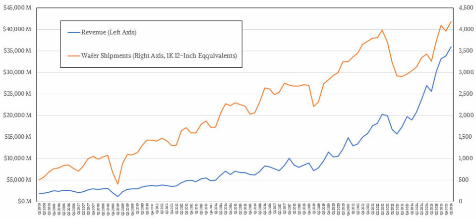
Measured in 12-inch (300mm) wafer terms across all the machines and various process nodes where TSMC is still etching chips, the foundry produced 4.17 million wafers in the third quarter of 2026, a record for the company, surpassing the 4.09 million wafers it produced in the third quarter of 2025. The wafer production rate in the March quarter was 28.1% higher than the same period last year. Continued at 5.4%. Of course, it’s difficult to know how many chips TSMC has produced, as chips come in a variety of shapes and sizes, ranging from tens to hundreds per wafer, but TSMC certainly knows this number and tracks it very closely as well.
Revenues earned per wafer have also increased, suggesting more complex chippers and the resulting packaging implied from acquiring high-end chips manufactured by TSMC. Just four years ago, TSMC’s average revenue per wafer was less than $5,000 (total revenue divided by 12-inch equivalent wafer production), but in the March quarter, revenue per wafer increased 1.7 times to $8,600 compared to four years ago. Revenue per wafer increased 9.8% year over year from the $7,832 level set in Q1 2025, but only increased 1% sequentially.
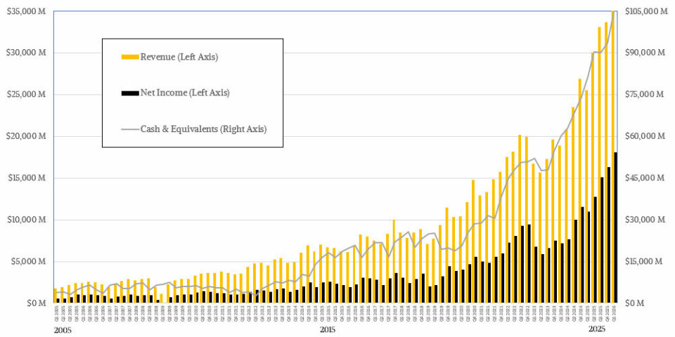
Adding up all those wafers and packages, TSMC posted sales of $35.9 billion in the March quarter, up 40.6% year over year, and net profit exploded 65.2% to $18.13 billion, accounting for 50.5% of revenue. TSMC is a capital-intensive and highly complex hardware maker with profit margins comparable to any software stack in history, including the venerable IBM mainframe, which remains afloat thanks to the tenacity of applications written over decades on System/360 and its successors.
Thanks to these strong profits, TSMC ended the quarter with $105.53 billion in cash and equivalent assets in the bank, but it only expects 2026 capital expenditures to be between $52 billion and $56 billion. TSMC just raised it to the “high end” of that range on a conference call with Wall Street analysts. That’s $56 billion. There’s no doubt that capex will increase next year and beyond, but it’s convenient that TSMC has nearly two years of capex in the bank, and that’s only at the beginning of this year.
But what can you really buy with that amount of money? According to TSMC, 70% to 80% of this year’s capital investment will be spent on foundries, which represents a combination of the expansion of the N3 node (3 nanometers) in Taiwan, the ramp-up of the N2 node (2 nanometers), and the start of the A14 node (1.4 nanometers), as well as the continued expansion of foundry operations that began several years ago in Arizona. Depending on who you ask, for a fab module that can process 50,000 wafer starts per month, a 3-nanometer fab module costs about $20 billion, a 3-nanometer module costs about $28 billion, and a 1.4-nanometer module costs about $49 billion. Instead of moving to a high NA process that significantly increases transistor density while cutting the reticle size in half, TSMC is doing a lot of additional patterning in their N2 and A14 processes, which means more equipment but less grief and change for customers.
TSMC’s total production capacity for monthly wafer shipments in 2025 “exceeded 17 million 12-inch wafer equivalents,” which was slightly higher than the level set for 2024. TSMC will certainly have another growth spurt, but it won’t and won’t be able to add so much production capacity that it won’t be able to pay the scarcity premium it enjoyed in 2025 into 2026 and beyond.
To be precise, even if TSMC could move faster, it probably won’t, given the state of the global economy and the concentration of GenAI spending among tech giants. There is little benefit to TSMC creating its own bankruptcy cycle. Especially if you’ve just come through a period in 2022 and 2023 when spending on PCs, smartphones, and general-purpose servers will all be down.
TSMC always talks about its business in terms of revenue by platform and revenue by process node, and we’re going to see those soon. But what everyone wants to know is how TSMC’s business is focused on chips for AI computing and networking, something the company has only hinted at. We calculated that based on how little TSMC has said in recent quarters.
First, revenue by process:
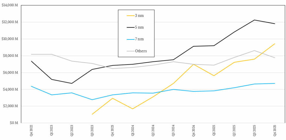
Volume production of the N5 process began about six years ago, and it remains the primary manufacturing process (along with the N4 variant) in the TSMC fleet, at least based on revenue, with first-quarter revenue of $12.92 billion, up 40.6 percent year-over-year and 9.5 percent sequentially. The N5/N4 nodes certainly don’t seem to have peaked. These are relatively cheap, high-yield manufacturing nodes, and there are plenty of chip companies holding back for these very reasons. Nvidia and AMD can charge a lot of money for CPUs and GPUs, which allows them to pay for the most advanced nodes.
The N3 node, which is several years younger, is here to stay, with revenue of just under $9 billion in Q1 2026, up 59.8% but down 5% sequentially. The much older N7 node (which also includes the N6 variant) is still not only doing well but growing, with sales increasing 21.9% to $4.67 billion. Sales for all other nodes (and many older nodes manufactured around the world) were $9.33 billion, up 35.4% in the March quarter. This kind of revenue is why the old Intel foundry model has moved away over the years. This is because Intel has leading edge captive customers and is not a merchant foundry. Intel would kill for a legacy business like that, and may even build one someday.
By splitting the revenue by product, we can start to focus on the AI part of TSMC’s action. As always, you need to be careful with terminology here. When TSMC says HPC, it means all kinds of high-performance chips used in PCs and servers, including CPUs, GPUs and XPUs, various types of switching and routing ASICs, and FPGAs.
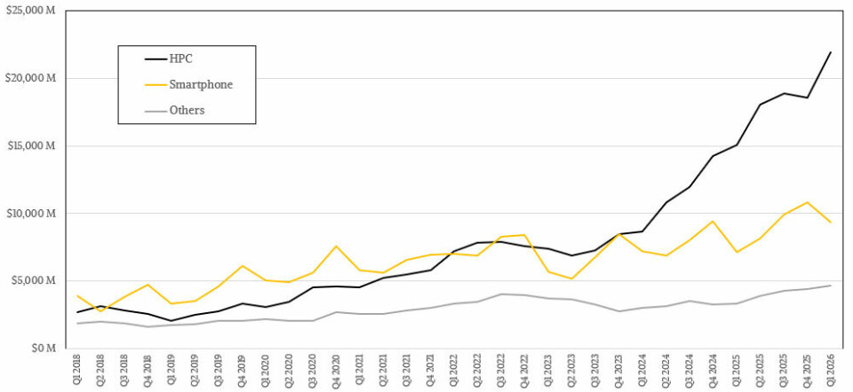
It’s been nine quarters since TSMC’s HPC division matched its smartphone division in terms of revenue. Currently, the HPC division, which posted revenue of $21.9 billion in Q1 2026, is more than twice the size of the smartphone division, which had revenue of $9.33 billion. As you can see, the HPC segment is growing faster, up 45.4 percent year over year and 18 percent sequentially, but I don’t think all of that growth is being driven by AI.
These days, a lot of high-end PC and server CPUs are made and sold out. The smartphone chip business grew a very healthy 30.6%, but I don’t think smartphones will ever catch up with HPC at TSMC again unless the GenAI bubble bursts. In fact, it is much more likely that TSMC will split HPC into AI and non-AI segments, as this is an important distinction that investors should be aware of.
This will give you this nice little graph.
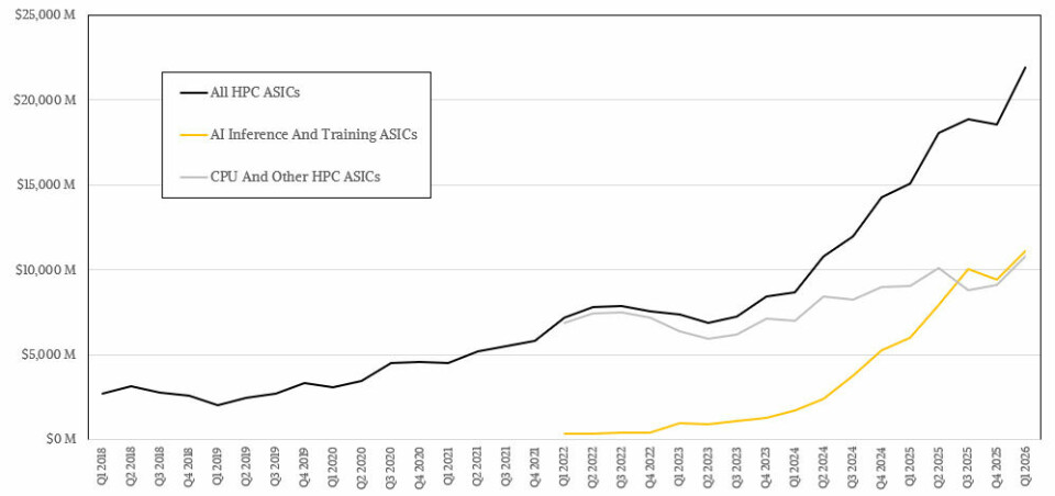
There’s a lot of magic involved, don’t get me wrong. However, the model is consistent with a long-term compounded annual growth rate that TSMC has set at “mid-to-high 50%” between 2024 and 2029. Its forecast was for a mid-40% CAGR in early 2025.
I said that the GenAI boom will eventually stop growing explosively, but it will still grow very quickly and be very large. And since this is the curve that new and explosive technologies follow, the model reflects this. Additionally, TSMC’s profits are driven more by supply than demand, and as mentioned above, it can’t build up too much production capacity even if it wanted to. And TSMC definitely doesn’t want that.
Back in 2022, TSMC’s AI business may have been worth just $1.52 billion, but it grew by triple digits every quarter from 2023 to 2024, reaching an impressive $33.38 billion in the first three quarters of 2025 for all of 2025. I think the growth rate in Q4 2025 and Q1 2026 was much slower. The year-on-year comparisons were % and 84.9%, respectively. But in the past two quarters, the AI chip business has accounted for just over half of overall TSMC HPC chip revenue, and by next quarter it will probably account for more than a third of TSMC’s overall revenue. (That doesn’t include AI PC CPUs or CPUs with matrix or vector engines; they may do AI on the side, but that’s not their primary purpose.)
In terms of numbers, I think the non-AI part of the TSMC HPC business grew 19.2% to about $10.8 billion, and the AI part grew 84.9% to about $11.1 billion.
That’s pretty surprising for a business that was interesting but not overwhelming just four years ago.