
Underived techniques to solve problems where gradient-based methods are lacking.

As semiconductor technology advances, device structures become more and more complicated. New materials and architectures introduce complex physical effects that require accurate modeling to ensure reliable circuit simulation and design. Correspondingly, these accuracy requirements increase the accuracy and efficiency of device modeling.
Modern device models often contain hundreds of interdependent parameters. Effects such as short channel behavior, mobility degradation, and self-heating are highly correlated, creating nonlinear parameter spaces that are difficult to optimize. Traditional optimizers are useful for local tuning, but are trapped in local minimal during global optimization, resulting in long, manual, and error-prone modeling flows.
To overcome these limitations, this blog explores how machine learning (ML) is revolutionizing the model extraction process. ML-based optimization efficiently navigates complex, multivariate parameter spaces, achieving better convergence and higher accuracy, and significantly less manual tuning and designer effort. ML opens the door to a more automated, robust and scalable modeling flow that meets today's fast-paced semiconductor technology.
Challenge: Complexity and correlation
The compact model relies on a number of parameters to simulate device behavior under a variety of conditions. For simple devices such as Schottky diodes, this may contain only three parameters. However, for modern devices such as Gan Hemts and Advanced CMOS transistors, the number of parameters can easily exceed hundreds.
In this environment, traditional gradient-based optimization algorithms such as Newton Rafson and Levenberg-Marquardt have stopped. These methods often:
- A careful first guess is required
- Degrades performance using many highly correlated parameters
- You'll be trapped in a local minimal
- Demand Manual Intervention and Iterative Tuning
As a result, engineers often spend days or weeks tweaking models without guaranteeing they will find the best global one.
Introducing the ML Optimizer
To address these limitations, KeySight is shifting towards gradient-free optimization algorithms. These methods are more robust to noise, suitable for non-convex states, and are independent of initial conditions.
Keysight has developed ML Optimizer. ML Optimizer is a machine learning-based solution designed specifically for compact model parameter extraction. It combines the strengths of a gradient-free method with adaptive learning to provide adaptive learning.
- Global optimization The entire high-dimensional parameter space
- Robust performance Even if the initial value is bad
- Support for over 40 parameters In a single step
The ML optimizer continuously learns from each iteration and improves strategies to balance exploration and exploitation. It is especially effective for automated extraction applications where stability and accuracy are important.
Both the IC‑ CAP gene optimizers and ML optimizers are powerful derivative-free technologies to solve the problem of a lack of gradient-based methods. Designed for continuous optimization, ML Optimizers generally outperform the genetic optimizer of speed and accuracy of convex problems. Automatically adapts step size and search direction, minimizing the balance between exploration and exploitation, achieving faster convergence in higher dimension spaces.
Actual results
The ML optimizer was applied to various device modeling scenarios.
- Gan Hemt (ASM-HEMT model): Optimize your DC module in one step using a 4×50μM device. A great fit achieved in less than 6,000 tests, resulting in an Id Only 1.25E-3 error.

- MOSFET Re-Centering (BSIM4): A model that meets the evolutionary process specifications with minimal manual adjustment.
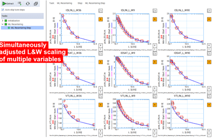
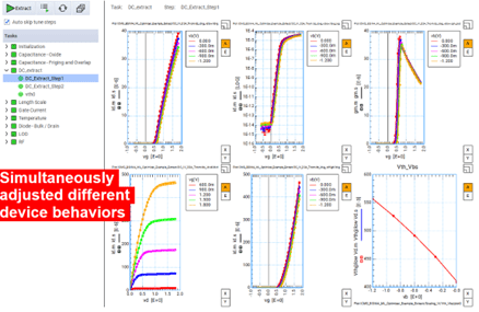
- MOSFET DC and CV fitting (BSIM4):Unified multiple plots and parameters become a single global optimization step, minimizing iterative cycles and improving overall accuracy.
- MOSFET DC and CV Fitting (BSIM4) – Advanced: This use case will be implemented in future Device Modeling MBP 2026, featuring an automatic extraction flow applied to over 40 devices. This process consists of four consecutive steps: a large device, an L-array, a W-array, and a small device. It fits accurately across a wide range of device operations and a wide range of device sizes.
New ML-enabled ERA for device modeling
both Device Modeling for IC-CAP 2025 and MBP 2026 Integrate new ML optimizers to dramatically simplify workflows, reduce human error, accelerate time to model, and allow for faster, more reliable passes to high-quality results.
Adding ML represents a major advance in device modeling. By leveraging machine learning, ML Optimizer offers:
- Fastest model development
- Better Global Optimal Solutions
- Minimum manual tuning
- More robust automatic modeling flow
As semiconductor technology continues to evolve, tools like ML optimizers are essential to meet design demands.
For more information, check out the demo video and application notes provided by Keysight.
yiao li
(All posts)
Yiao Li is an application developer for Keysight Technologies.


