There is a limit to how fast copper wires can move data between computers, and moving to the speed of light will ultimately advance AI and high-performance computing. All major chip makers agree that optical interconnects will be needed to reach zettascale computing in an energy efficient manner. Last month, her CEO of AMD, Lisa Su, shared this opinion.
Google has experimented with and deployed optical interconnects between servers and chips in their data centers. In an arXiv paper published last week, the company shared details about its implementation and its performance and power efficiency improvements.
Google talked about its TPU v4 supercomputer with 4,096 Tensor Processing Units (TPUs). Google runs its AI applications on his TPU chips, including Bard, an early iteration of the company’s AI-infused search engine. The company deploys dozens of his TPU v4 supercomputers on Google Cloud.
Google’s paper on supercomputing infrastructure comes after Microsoft made a fuss about the Nvidia GPU-powered Azure supercomputer powering ChatGPT. By comparison, Google was conservative about introducing AI into his web applications, but now Bing search engine he is trying to catch up with Microsoft introducing his GPT-4 large language model of OpenAI. increase.
Optical connections have been used for decades for long-distance communication over telecommunication networks, but are now considered suitable for short-distance use in data centers. Companies such as Broadcom and Ayar Labs create products for optical interconnects.
Google’s TPU v4 supercomputer was introduced in 2020. This paper is written as a retrospective article measuring performance improvements over time.
Supercomputer is ‘first with circuit-switched optical interconnect,’ says Google researchers HPC wire on mail.that There were a total of 64 racks hosting 4,096 TPUs and 48 optical line switches connecting all racks throughout the system. Google calculated that optical components account for less than 5% of the system cost and less than 2% of the power consumed by the system.
Google researchers wrote that TPU v4 chips are 2.1 times better than TPU v3 chips and offer 2.7 times better performance per watt. “The TPU v4 supercomputer is four times bigger than he is on a 4096 chip, and therefore up to 10 times faster overall, which lends itself to large-scale language models, along with the flexibility of OCS,” the researchers wrote in their paper. .
Google emphasized the flexibility of the optics when deploying the system and adapting the topology on-the-fly according to the application. tThe optical interconnect and its high bandwidth allowed each rack to be deployed independently and connected once production was complete.
“The gradual deployment has significantly improved time-to-production and greatly improved the cost-effectiveness of the TPU v4 supercomputer,” said the researchers.
The predecessor TPU v3 supercomputer, with a total of 1,024 TPU chips, was a different story altogether. “The TPU v3 system was unusable until all 1,024 chips and all cables were installed and tested. Any delay in delivery of any component would have stalled the entire supercomputer,” the researchers wrote. increase.
Google described the company’s optical circuit switching as a next-generation interconnect, comparing it to Nvidia’s NVSwitch, which is based on electrical engineering. An optical switch is “fibers connected by mirrors, so the bandwidth running over the fiber can now be switched between input and output fibers by OCS across 4,096 chips,” Google researchers said. said.
The interconnect is scalable to more TPU cores and can establish links at terabits per second.
The research paper compared the TPU v4 chip to Nvidia’s A100 chip, which is still in use in 2020 and is manufactured using the 7nm process. Nvidia’s recent Hopper H100 wasn’t available in the cloud until earlier this year. Google has left open the option of comparing the next-generation of his TPU v5 to his H100.
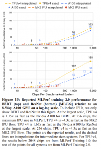
Google claimed that its chip could outperform the A100 and Graphcore AI chips, but researchers have also voiced their opinions on AI benchmarks such as MLPerf, which measures peak training and inference performance. Google researchers claim that the TPU v4 chip enabled better and better use of computing resources in real-world scenarios.
“The HPC community is familiar with the gap between Linpack performance and the performance offered in real-world applications, and the ACM Gordon Bell Award recognizes it. We achieved 5% to 10% of Linpack flops/sec.As mentioned in the paper, peak times and delivered AI performance are not necessarily correlated.Large language models are We are proud to have trained at an average of 58% of peak hardware performance on TPU v4 over 50 days.”
TPU v4 supercomputers include SparseCores, intermediate chips close to high-bandwidth memory where much of the AI processing takes place. The SparseCores concept supports new computing architectures being researched by AMD, Intel, Qualcomm, and others. It relies on data-close computing and orchestration between data movement in and out of memory.
The paper spends a lot of time on performance and energy efficiency metrics comparing the TPU v4 supercomputer to Nvidia’s A100. Still, Google generally optimizes applications for processing on TPUs.
Google The company has used the optical circuit switch detailed in last year’s paper for other applications, but this is the first time it has created a large-scale optical interconnect.