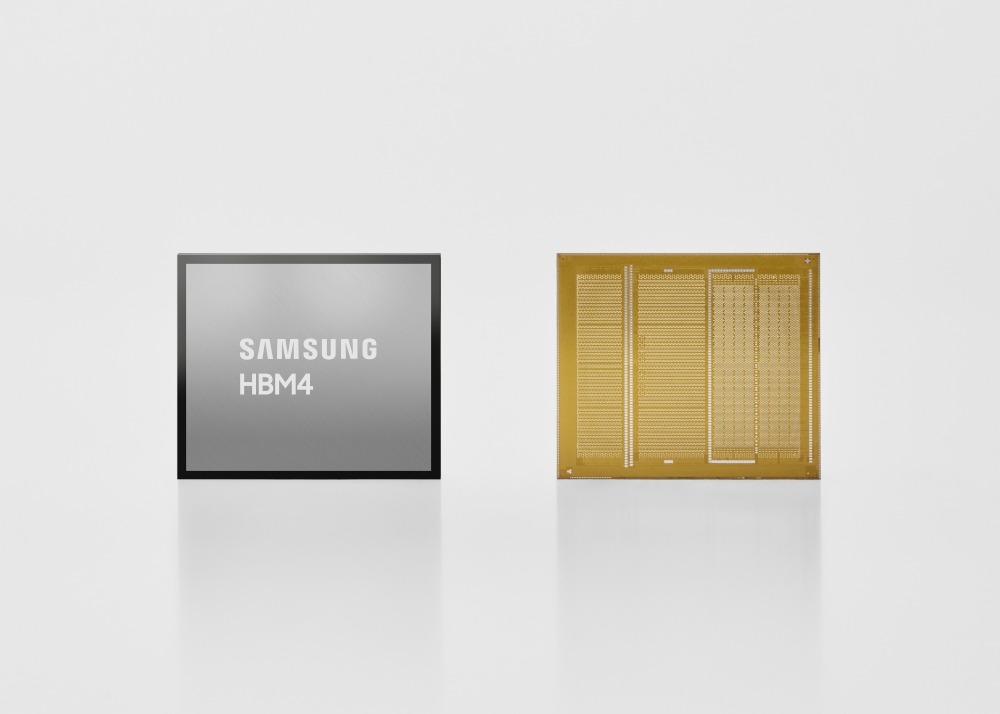
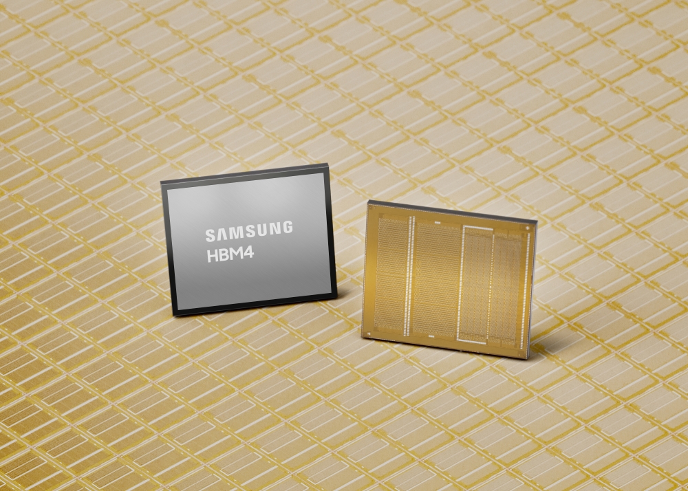
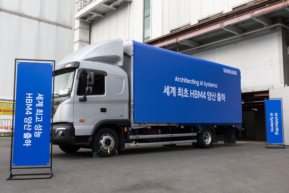
Samsung Electronics, a global leader in advanced memory technology, today announced that it has begun mass production of its industry-leading HBM4 and has shipped commercial products to customers. This achievement is an industry first and secures an early leadership position in the HBM4 market.
The company has achieved stable yields and industry-leading performance from the start of volume production by aggressively leveraging the state-of-the-art 6th generation 10 nanometer (nm) class DRAM process (1C). All of this was achieved seamlessly without any additional redesign.
“Instead of taking the traditional path of leveraging existing, proven designs, Samsung has taken the plunge and adopted cutting-edge nodes such as 1c DRAM and 4nm logic processes for HBM4,” said Sang Jun Hwang, executive vice president and head of memory development at Samsung Electronics. “By leveraging our process competitiveness and design optimizations, we are able to secure significant performance headroom, allowing us to meet our customers’ increasing performance demands when they need it.”
Setting standards for maximum performance and efficiency
Samsung’s HBM4 delivers a stable processing speed of 11.7 gigabits per second (Gbps), approximately 46% faster than the industry standard of 8 Gbps, setting a new benchmark for HBM4 performance. This represents a 1.22x increase over the previous generation HBM3E’s maximum pin speed of 9.6Gbps. HBM4’s performance can be further enhanced up to 13Gbps, effectively mitigating data bottlenecks that grow as AI models continue to scale up.
Additionally, the total memory bandwidth per single stack is increased by 2.7x compared to HBM3E, up to 3.3 terabytes per second (TB/s).
With 12-layer stacking technology, Samsung offers HBM4 in capacities ranging from 24 gigabytes (GB) to 36 GB. The company also keeps capacity options in line with future customer timelines by leveraging 16-tier stacking, scaling its products up to 48 GB.
To address the power and thermal challenges posed by doubling data I/O from 1,024 to 2,048 pins, Samsung has integrated advanced low-power design solutions into the core die. HBM4 also leverages low-voltage through-silicon via (TSV) technology and power distribution network (PDN) optimization to improve power efficiency by 40%, while increasing thermal resistance by 10% and heat dissipation by 30% compared to HBM3E.
Samsung’s HBM4 brings superior performance, energy efficiency, and high reliability to future data center environments, enabling customers to achieve maximum GPU throughput and effectively manage total cost of ownership (TCO).
Comprehensive yet agile production capabilities
Samsung is committed to advancing its HBM roadmap through comprehensive manufacturing resources, including the industry’s largest DRAM production capacity and dedicated infrastructure, to ensure a resilient supply chain capable of meeting the expected surge in HBM4 demand.
Tightly integrated design technology collaborative optimization (DTCO) between the company’s foundry and memory businesses ensures the highest standards of quality and yield. Additionally, our extensive in-house expertise in advanced packaging allows us to streamline production cycles and shorten lead times.
Samsung also plans to expand the scope of its technology partnerships with key partners based on close discussions with global GPU manufacturers and hyperscalers focused on next-generation ASIC development.
Samsung expects HBM sales to more than triple in 2026 compared to 2025 and is actively expanding HBM4 production capacity. Following the successful market introduction of HBM4, sampling for HBM4E is expected to begin in late 2026, while custom HBM samples are expected to begin reaching customers in 2027 according to their specifications.