
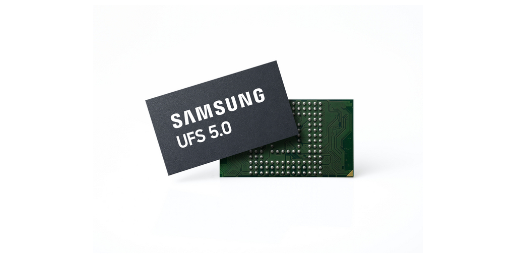
Seoul, South Korea–(BUSINESS WIRE)–Samsung Electronics Co., Ltd., a global leader in advanced memory technology, today announced that, for the first time in the industry, it has developed the industry’s fastest Universal Flash Storage (UFS) 5.0 solution that will help enable seamless and highly efficient AI services on future mobile devices.
“In the era of on-device AI, storage devices are evolving into a key driver in defining the AI experience,” said Jangseok Choi, head of memory product planning at Samsung Electronics.
share
This milestone sets a new benchmark for the next generation mobile memory market. This is expected to allow mobile device users to experience significantly lower latency and significantly faster response times when running large-scale language models (LLMs) in on-device AI environments.
“In the era of on-device AI, storage devices are evolving into a key driver in defining the AI experience,” said Jangseok Choi, head of memory product planning at Samsung Electronics. “By successfully progressing through the development stage of the industry’s first UFS 5.0 solution, Samsung sets a new standard for on-the-go storage and continues to drive innovation in the next-generation mobile platform market.”
Generative AI is rapidly moving from the cloud to devices, and the scale of data required for local processing is rapidly increasing. As a result, storage is evolving from a medium primarily used to store data to a core infrastructure that supports AI computations.
Samsung’s UFS 5.0 integrates JEDEC’s latest embedded memory interface standard to deliver unparalleled performance levels with industry-leading bandwidth of up to 10.8 gigabytes per second (GB/s).
The new storage solution delivers sequential read speeds of up to 10.8 GB/s and sequential write speeds of up to 9.5 GB/s, each more than twice as fast as the previous UFS 4.1 standard. This significant advance significantly speeds up large-scale data storage and processing for on-device AI applications.
The power efficiency of Samsung’s UFS 5.0 is also improved by more than 40% compared to the company’s UFS 4.1 solution. This is achieved by implementing many new innovations such as clock gating and multi-voltage technology. These enhancements significantly reduce the power required to transfer the same amount of data, significantly reducing overall power consumption and extending battery life for next-generation mobile devices.
Samsung designed the UFS 5.0 solution into an ultra-small package measuring just 7.5 mm x 13 mm x 0.9 mm, making it 16.7% smaller than the previous generation. This form factor greatly increases design flexibility and internal space utilization for a wide range of applications including mobile, wearable, and augmented reality (XR) devices.
Samsung plans to begin mass production of UFS 5.0 in various capacities up to 1 terabyte (TB) in the fourth quarter of this year. With this breakthrough in UFS 5.0 technology, Samsung plans to stay ahead of industry needs and expand its supply as the next-generation device market grows, from flagship smartphones to XR headsets and AI wearables.
About Samsung Electronics Co., Ltd.
Samsung inspires the world and shapes the future with innovative ideas and technology. The company is redefining the world of televisions, digital signage, smartphones, wearables, tablets, consumer electronics, and networking systems, as well as memory, system LSI, and foundry. Through HARMAN, Samsung also creates innovative automotive and audio products while advancing medical imaging technology, HVAC solutions, and robotics. With our SmartThings ecosystem, open collaboration with partners, and AI integration across our portfolio, Samsung delivers seamless and intelligent connected experiences. For the latest news, visit Samsung Newsroom (news.samsung.com).


