With the HBM4 ERA preparing for the horizon and SK Hynix and Micron for production ramp-ups from late 2025 to 2026, it is an ideal time to explore how HBM (high-bandwidth memory) is built, why its important benefits and technology are relevant, and why its manufacturing complexity leads to high costs. Here's a quick summary of the essential points.
Internal HBM: Configuration and Important Benefits
As AI models are more refined, processing both intensive training and real-time inference demands memory that can be delivered in three dimensions: size, speed and efficiency. SRAM is fast, but lacks capacity, while traditional DRAM provides ample storage, but lacks sufficient bandwidth. The HBM emerges as a sweet spot, providing the optimal balance between capacity and speed.
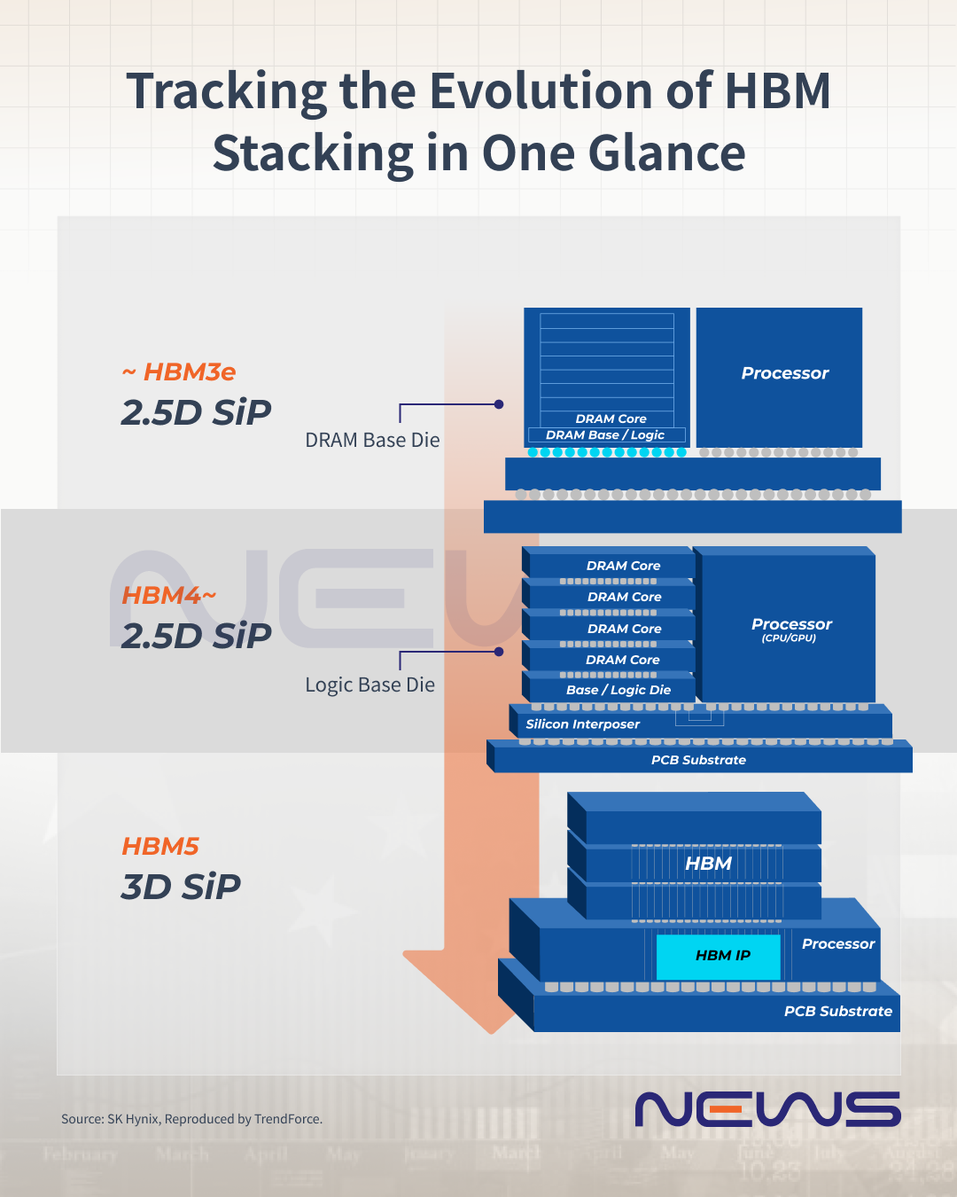
HBM achieves this through its own stacked architecture. Multiple DRAM dies are constructed, built on top of logic (base) dies, connected through thousands of parallel interconnects. This entire stack links to the XPU via a silicon interposer on the package board. It usually pairs with a GPU like Nvidia.
This architecture offers several important benefits. First, energy efficiency: tight integration between the HBM and XPU reduces data paths and reduces power consumption. Secondly, huge throughput.
In comparison, HBM4s typically use 40-50% less power than DDR4 to achieve the same bandwidth. The DDR4 module is at a maximum of approximately 25.6 GB/s, while a single HBM4 stack offers bandwidth of 1 TB/s or more. This is a huge boost that is essential for workloads that require rapid access to large datasets.
Break the memory wall: Why HBM moves the AI era
In the age of generation AI, training models at the scale of ChatGPT typically requires tens of thousands of GPUs to run simultaneously. However, GPU computing power has increased 60,000 times over the last 20 years, while DRAM memory bandwidth has only improved by 100 times. It creates what is known as a “memory wall.” Simply put, no matter how fast the GPU is processed, if the memory cannot provide data quickly enough, then a bottleneck is acquired.
The HBM has its vertical stacking structure and was developed precisely to break through this barrier. It's like a skyscraper, with layers of drum tips stacked on top. Technically, each DRAM die has a thickness of about 30-50 µm, connected to the underlying logic base via Sillicon Vias (TSVS) and Microbumps, and ultimately linked to the GPU via a silicon interposer.
This architecture allows HBMs to simultaneously transmit data over thousands of “fast channels” and provide well beyond the bandwidth of traditional DDR memory.
Innovation Price: HBM Engineering Challenges
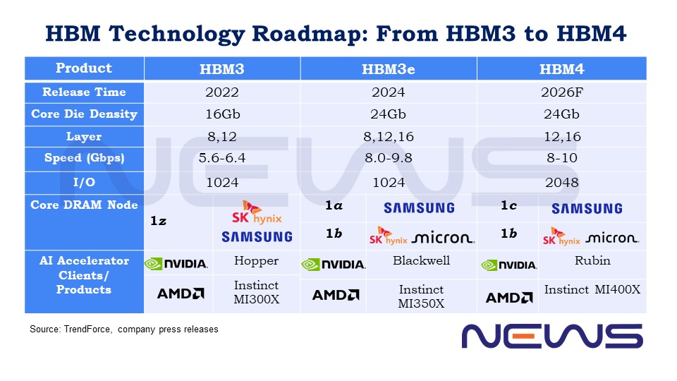
However, building a skyscraper like this is extremely expensive. According to Trendforce, the HBM3E is already on sale at an estimated 20% price premium, and the additional complexity of the HBM4 is expected to push that premium by more than 30%.
The higher cost, the Trendforce note comes from the more complex chip design of the HBM4 and expands the die size to accommodate a significant increase in I/O count. Additionally, some manufacturers have moved to logic-based base die architectures to further improve performance, with both factors contributing to more sudden production costs.
In particular, the complexity of stacking continues to be a major hurdle for each new generation of HBMs. When the layer increases to 12 or 16, TSV yield becomes a critical bottleneck.
Different manufacturers have adopted different approaches to address these challenges. SK Hynix took the lead by leveraging MR-MUF (Mass Reflow Molding Underfill) technology, but Samsung and Micron continue to rely on the TC-NCF (thermal compression with non-conductive film) method.
According to Sk HynixMR-MUF, which has been applied to its HBM2 products since 2019, has set up a company other than competitive. This technology works like a “2-inch” process that combines chip connection and protective filling in one step. The traditional approach is like building a house first and then patching the cracks, but Mr-Muf is like sealing the cracks as you build.
Simply put, mass reflow melts the bumps between stacked chips to connect them, while molded underfill fills the gaps with protective materials that help to increase durability and dissipate heat. This combined approach is particularly effective for high-rise, high-bandwidth applications with strict thermal requirements such as HBMs.
Compared to NCF, MR-MUF offers about twice the thermal conductivity. This has a major impact on both production speed and yield.
However, hybrid bonding excludes thin stacks, more layers, reduced signal loss and better yield by connecting the chips directly without bumps. Therefore, major HBM manufacturers are considering whether to adopt hybrid bonding for HBM4 16HI stack products, but have confirmed plans to implement this technology in HBM5 20HI stack generation.
HBM4 Base Die: Why Memory Makers Turn to Foundry
Nevertheless, stacking drum layers is just the beginning. The next challenge is to build them on a very accurate and deep foundation.
This is extremely important in the HBM4 era. Products require a specialized foundation known as The Logic Die. This foundation, surprisingly, needs to handle over 2,000 accurate connection points (1,024-2,048 I/O counts). Imagine this a building that requires 2,000 separate utility lines.
Traditional memory makers accustomed to building “homes” (standard memory) suddenly face the near impossible task of building foundations for these super-deep skyscrapers. They turn to foundries with expertise, like TSMC, as they simply buy billions of dollars with ultra-precision excavation equipment to occasionally dig such foundations.
Take TSMC as an example. As pointed out TechnologyFoundry Giant owns cutting-edge tools (N5 and N12FFC+ processes) to allow the N12FFC+ process to build 12 stack (48GB) or 16 stack (64GB) memory “building” with data transfer speeds such as the installation of a Super Speed elevator. Meanwhile, the N5 process offers even more accuracy at 6-9 micrometer intervals, allowing direct bonding technology that allows memory stacks to be built directly on top of logic chips.
HBM: It's still an oliopoly game
One thing is clear as Memory Giants prepares for the HBM4 ERA and races to ensure Nvidia validation. Trendforce will lead with 59% shipments in 2025, with Samsung and Micron holding around 20% each.
In the upcoming HBM4 Battlegrounds, Nvidia and AMD will remain heavyweights, driving demand for memory giants. Nvidia has unveiled the next generation of Rubin GPUs at this year's GTC, but AMD is preparing the MI400 series as a direct competitor.
In terms of specifications, each DRAM die on an HBM is typically built from 4, 8, or 12 dies, typically 30-50 µm thick. Jedeck We observed a relaxed nominal package thickness of 775 µm on both the 12 and 16 height HBM4 stacks, elevated from 720 µm of the HBM3.
Meanwhile, the HBM4 doubles the I/O count from 1,024 to 2,048 compared to the previous generation, but maintains data transfer speeds above 8.0 Gbps, comparable to the HBM3E. This means that the HBM4 can provide twice the data throughput at the same speed due to increased channel count.
Foundries like TSMC play an increasingly important role as logic is at the heart of collaboration. It appears in HBM4's SK Hynix and HBM4E's Micron, making the battlefield of HBM4 more dynamic and unpredictable than ever before.
(Photo credit: SK Hynix)
Please note that this article quotes information. from Jedeck, Technology and Sk Hynix.

Next article
[News] Will investment be rewarded? Trillions have been poured into AI, but chips are reportedly only lasting 3-5 years