The results of this study were structured in distinct subsection, each addressing a particular aspect, including the impact of employing different charge transport layers, the effect of thickness and defect densities, and the impact of doping density on the performance of the proposed PSC. Additionally, the influence of the metal rear electrode and parasitic resistance on the effectiveness of the proposed PSC was investigated.
Simulation results validation
The reliability of the employed model and the accuracy of the SCAPS-1D analysis introduced in this work were validated by reproducing the study on the fabricated device proposed by Lu et al. 51 and subsequently evaluating the simulated results against the published ones. The simulated J-V response of the single-absorber MAPbI3 device exhibits strong agreement with the experimental data, as the achieved accuracy is greater than \(96 \%\). Only minor deviations were observed in the electrical performance, as JSC slightly dropped from \(22.9\) to \(22.82\ mA/c{m}^{2}\), and PCE shifted from \(20.8\) to \(20.88 \%\). The minor reduction in the VOC value from \(1.15\ V\) in the reported results to \(1.11\ V\) in the simulated results can be attributed to the simulator’s inability to capture all fabricated and environmental factors, even with the simulated structure being carefully adjusted to ensure strong agreement with reported findings. This performance demonstrates the reliability of the software. The complete input data and output electrical parameters are listed in Tables S5 and S6 of the Supplementary Information, respectively.
Impact of utilizing different HTLs on device performance
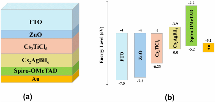
Transport materials can play crucial roles in suppressing ion migration, preventing perovskite degradation, and protecting the absorber layers from moisture and oxygen during prolonged exposure to light, air, and heat. Therefore, the choice of charge transport materials with optimal characteristics may be considered a critical aspect for escalating both stability and PCE of the device. The study started with the selection of the optimal HTL using the initial device configuration shown in Fig. 1(a) by considering several widely employed HTLs such as Spiro-OMeTAD, Cu2O, P3HT, CuI, CuO, CFTS, CBTS, PTAA, MoO3, PEDOT: PSS, MoS2, Cu2Te, nPB, and Sb2S3. The key electrical characteristics of the utilized HTLs are provided in Table S1 of the Supplementary Information, while the corresponding energy band alignments with the lower Cs2AgBiI6 absorber are indicated in Fig. 2.

The alignment of energy bands of the different utilized HTLs with the lower Cs2AgBiI6 absorber.
A systematic batch analysis was performed to identify the optimum HTL configuration, that improves the performance of the proposed device. The study examined the effect of thickness, acceptor, and defect concentrations of each utilized material on the effectiveness of the introduced device. Specifically, the HTL thickness was varied between \(50\) and \(500 nm\), the acceptor density ranged between \(1\times {10}^{15}\) and \(1\times {10}^{21\ }{ cm}^{-3}\), and the defect concentration ranged between \(1\times {10}^{11}\) and \(1\times {10}^{16}{\ cm}^{-3}\). Figures S1-S3 of the Supplementary Information present the effect of the examined parameters on the performance, whereas Table 3 reports the electrical characteristics associated with the maximum performance achieved when employing different HTLs with their optimized thickness, doping, and defect densities.
Changing the HTL influences the performance of PSC, as demonstrated by the results presented in Table 3. This variation in performance can be interpreted by many factors governing the transport and extraction of carriers, including the HTL alignment with the perovskite absorber, which can be expressed in terms of the valence band offset (VBO), which can be numerically determined as follows 52:
$$VBO={E}_{VB, Lower Absorber}-{E}_{VB,HTL}$$
(6)
here, \({E}_{VB, Lower Absorber}\) and \({E}_{VB, HTL}\) are the valence band (VB) edge energies of the Cs2AgBiI6 layer and the HTL, respectively. When the VB of the absorber is above that of the HTL, positive VBOs, or spikes, are introduced at the interface, which impede hole flow in the desired direction toward the HTL 45. Materials with a negative VBO, with HTL VB laying above that of the absorber, create energy cliffs. This generally facilitates hole transport into the HTL making such materials favorable. Nevertheless, an excessively large cliff may increase carrier recombination and reduce device performance 53. Accordingly, the utilization of PEDOT: PSS and CFTS as HTLs declines the performance of the suggested device as a consequence of their VBO values of \(-0.5\ eV\) and \(-0.9\ eV\), respectively, which are considered to be relatively high cliffs at the interface of the lower Cs2AgBiI6 absorber. It is noteworthy that the small positive VBO spikes of \(0.08\ eV\) and \(0.1\ eV\) at the lower absorber interface with CuO and Cu2O HTLs have minimal impact on performance, yielding PCE values of \(20.58 \%\) and \(20.51 \%\), respectively. On the other hand, employing HTLs with moderate VBO cliff values enhances the performance of the proposed device, as utilizing Sb2S3 (\(-0.18\ eV\)) and P3HT (\(-0.3\ eV\)) increases the PCE to \(21.83 \%\) and \(21.33 \%\), respectively. The results also reveal that Sb2S3 achieved the highest performance among all other utilized HTLs in this study.
Figures 3–5 present the influence of changing the thickness, defect, and the acceptor doping densities of Sb2S3 HTL, respectively, on the proposed dual-absorber PSC performance. As illustrated in Fig. 3, increasing the Sb2S3 HTL thickness from \(50\) to \(500\ nm\) enhances performance. Specifically, JSC rises by \(5.34 \%\) from \(23.03\) to \(24.26\ mA/{cm}^{2}\) as thickness increases to \(500\ nm\).

The effect of thickness variation of the Sb2S3 layer on the proposed dual-absorber PSC’s performance.
In contrast, the value of VOC is almost unaffected, maintaining a constant value near \(1.1 V\). The PCE of the proposed structure rises from \(20.77\) to \(21.83 \%\) as the HTL thickness elevates from \(50\) to \(500\ nm\), while the FF reduced by \(0.33 \%\) over the same thickness range.
The defect density of the Sb2S3 HTL showed a slight impact on the performance of the proposed cell. As shown in Fig. 4, increasing the Sb2S3 layer’s defect density from \(1\times {10}^{11}\) to \(1\times {10}^{16} {\ cm}^{-3}\) induces a minor reduction in the effectiveness of the suggested PSC. In detail, the value of JSC is kept constant at \(24.26\ mA/{cm}^{2}\) while changing the defect concentration from \(1\times {10}^{11}\) to \(1\times {10}^{14} {\ cm}^{-3}\), then it slightly reduces to \(24.25\ mA/{cm}^{2}\) and \(24.18\ mA/{cm}^{2}\) with the increase in the bulk defect concentration to \(1\times {10}^{15} {\ cm}^{-3}\) and \(1\times {10}^{16} {\ cm}^{-3}\), respectively. Furthermore, the PCE value only reduces by \(0.08 \%\) upon the increase of defect concentration to \(1\times {10}^{16} {\ cm}^{-3}\). In addition, the values of VOC and FF are almost unaffected by the Sb2S3 layer’s defect density variation over the employed range, keeping their values almost constant at \(1.1\ V\) and \(81.87 \%\), respectively.

The effect of defect density variation of the Sb2S3 layer on the proposed dual-absorber PSC’s performance.
The density of acceptor atoms in the Sb2S3 HTL, on the other hand, has a considerable impact on the performance of the proposed device. A strong influence on the strength of the electric field at the HTL/absorber interfaces is induced by the doping concentration within the HTL which makes it a critical parameter for device performance. The enhanced electric field promotes more effective separation of the generated electron- hole pairs, which increases the overall performance 54. As indicated by Fig. 5, increasing NA of Sb2S3 from \(1\times {10}^{15}\) to \(1\times {10}^{16} {\ cm}^{-3}\) diminishes JSC by \(0.98 \%\), reducing its value from \(24.25\) to \(24.21\ mA/{cm}^{2}\), then it shows a slight increase to \(24.26\ mA/{cm}^{2}\) upon rising the acceptor density to \(1\times {10}^{21} {\ cm}^{-3}\). The value of VOC rises by \(4.55 \%\) from \(1.05\ V\) at doping concentration of \(1\times {10}^{15} {\ cm}^{-3}\) to \(1.1\ V\) at NA of \(1\times {10}^{21} {\ cm}^{-3}\). Further, the values of PCE and FF increase with the Sb2S3 layer’s acceptor doping density increase, achieving the maximum PCE of \(21.83 \%\) and FF of \(81.87 \%\), at an Sb2S3 doping density of \(1\times {10}^{21} {\ cm}^{-3}\).

The effect of doping density variation of the Sb2S3 layer on the proposed device’s performance.
Impact of utilizing different ETLs on device performance
The investigation was extended to identify the optimal ETL, using the initial device configuration shown in Fig. 1(a), while substituting the HTL with Sb2S3, which was shown in the preceding subsection to be the most effective HTL among the evaluated candidates. Several common electron transport materials were assessed including TiO2, PCBM, C60, IGZO, SnO2, WS2, SnS2, CdS, ZnSe, PC60BM, LBSO, Nb2O5, and CdZnS. The main electrical characteristics of the employed ETLs are provided in Table S2 of the Supplementary Information, while the corresponding energy band alignments with the upper Cs2TiCl6 absorber are indicated in Fig. 6.

The alignment of energy bands of the different utilized ETLs with upper Cs2TiCl6 absorber.
To determine the optimum ETL configuration, which escalates device performance, another systematic batch analysis was performed. The investigation examined the influence of thickness, donor doping, and defect concentrations of each utilized material on the proposed device performance. Specifically, the ETL thickness was varied from \(50\) to \(500\ nm\), the donor doping concentration ranged between \(1\times {10}^{15}\) and \(1\times {10}^{20}{\ cm}^{-3}\), and the density of bulk defects ranged between \(1\times {10}^{11}\) and \(1\times {10}^{16}{\ cm}^{-3}\). Figures S4-S6 of the Supplementary Information present the impact of the examined parameters on the performance, whereas Table 4 reports the electrical characteristics associated with the maximum performance achieved when employing different ETLs with their optimized thickness, doping, and defect densities.
Changing the ETL clearly affects the performance of PSC, as indicated by the results presented in Table 4. This variation in performance can be interpreted by many factors governing the transport and extraction of carriers including the amount of absorbed light within the ETL and its absorption coefficient in addition to the alignment of the ETL with the upper absorber layer which can be expressed in terms of the conduction band offset (CBO) which can be determined at the interface of the ETL as follows 52:
$$CBO={E}_{CB,ETL}-{E}_{CB, Upper Absorber}$$
(7)
where, \({E}_{CB,Upper Absorber}\) and \({E}_{CB, ETL}\) denote the edge energies of conduction bands (CBs) of the Cs2TiCl6 layer and the ETL, respectively. Positive CBOs or spikes are created when the CB of the ETL lies above the absorber’s CB, leading to resistance of the electron flow in the desired direction into ETL 45.
On the other hand, materials with negative CBO with CB of the ETL laying below that of absorber create energy cliffs with absorber layer, which generally facilitates electron transport into ETL making such materials favorable. Nevertheless, excessively large cliffs increase carrier recombination which leads to device performance deterioration 53. Therefore, employing ETLs that create positive CBO spikes at the interface with the upper Cs2TiCl6 absorber, such as C60 (\(0.1\ eV\)) and WS2 (\(0.05\ eV)\) reduces the device PCE to \(17.6 \%\) and \(18.37 \%\), respectively. Further, utilizing materials that create significant energy cliffs at the interface with upper absorber negatively affects the device effectiveness, resulting in PCE values of \(19.9 \%\) for CdS (\(-0.5\ eV\)) and \(19.26 \%\) for LBSO (\(-0.4\ eV\)). In contrast, using ETLs with moderate CBO cliff values escalates the performance of the introduced PSC as shown by the escalated PCE when SnS2 (\(-0.26\ eV\)) and ZnSe (\(-0.09\ eV\)) were employed. The results also indicates that SnS2 achieves the highest performance among the investigated ETLs in this study.
Figures 7–9 illustrate the influence of varying thickness, defect density, and the donor doping density of SnS2 ETL on the effectiveness of the introduced Cs2TiCl6– Cs2AgBiI6 half tandem device. As presented in Fig. 7, rising the thickness of the SnS2 ETL from \(50\) to \(500\ nm\) slightly escalates performance of the Cs2TiCl6-Cs2AgBiI6 proposed PSC. Particularly, JSC increases by \(0.82\%\) from \(24.3\) to \(24.5\ mA/{cm}^{2}\) while elevating the thickness to \(500\ nm\). In addition, VOC exhibits negligible variation, remaining essentially constant around \(1.1\ V\). Further, PCE of the proposed PSC rises from \(21.76\) to \(22.15 \%\) as the ETL thickness increases from \(50\) to \(500\ nm\), while the value of FF increases from \(81.36\) to \(82.03 \%\) over the same thickness range.

The effect of thickness variation of the SnS2 layer on the proposed dual-absorber PSC’s performance.
On the other hand, the bulk defect concentration of the SnS2 ETL has a more significant effect on the performance of Cs2TiCl6-Cs2AgBiI6 proposed device. Defects in ETL, which can be originated from structural dislocations, native imperfection, or contamination by foreign atoms, contribute to the creation of both shallow and deep traps. As indicated in Fig. 8, increasing concentration of defects of the SnS2 ETL from \(1\times {10}^{11}\) to \(1\times {10}^{16} {\ cm}^{-3}\) causes a tremendous reduction of the proposed PSC performance. In detail, JSC reduces from \(24.5\) to \(10.78\ mA/{cm}^{2}\) with the increase of the defect density of the SnS2 layer from \(1\times {10}^{11}\) to \(1\times {10}^{16} {\ cm}^{-3}\). Furthermore, VOC decreases by \(2.73 \%\) from \(1.1\) to \(1.07\ V\) due to escalating Nt from \(1\times {10}^{11}\) to \(1\times {10}^{16} {\ cm}^{-3}\). In addition, the value of PCE faces a massive reduction of \(12.97 \%\) upon the increase of defect density to \(1\times {10}^{16} {\ cm}^{-3}\). Also, the value of FF was influenced by the variation of SnS2 layer’s defect concentration over the employed range. Increasing Nt of the SnS2 layer from \(1\times {10}^{11}\) to \(1\times {10}^{14} {\ cm}^{-3}\) results in \(7.72 \%\) reduction of FF. Beyond that, FF starts to rise in correspondence with the increase of defect density.

The effect of defect density variation of the SnS2 layer on the proposed dual-absorber device’s performance.
Additionally, the donor doping density of SnS2 layer has considerable influence on performance. As indicated by Fig. 9, increasing ND of SnS2 layer from \(1\times {10}^{15}\) to \(1\times {10}^{20} {\ cm}^{-3}\) has a negligible impact on JSC, as it remains essentially constant around \(24.5\ mA/{cm}^{2}\). The value of VOC slightly reduced by \(0.01\ V\) from \(1.11\ V\) at doping density of \(1\times {10}^{15} {\ cm}^{-3}\) to \(1.1\ V\) at \(1\times {10}^{20} {\ cm}^{-3}\). Further, values of PCE and FF were escalated as result of increasing SnS2 doping density, achieving maximum PCE and FF values of \(22.15 \%\) and \(82.03 \%\), respectively, with SnS2 layer’s doping density of \(1\times {10}^{20} {\ cm}^{-3}\).

The effect of doping density variation of the SnS2 layer on the proposed dual-absorber device’s performance.
Structural optimization of proposed dual-absorbers
In the following subsections, the effects of variations in the thickness, bulk defect, and doping densities of photo-absorber layers on the performance of the Cs2TiCl6-Cs2AgBiI6 bi-absorber proposed PSC are analyzed. The device is configured with Sb2S3 and SnS2 as HTL and ETL, respectively, based on their superior effectiveness among the examined CTLs. The aim of this part of the study is to optimize the device performance and maximize the PCE of the proposed device.
Effect of thickness variation of upper absorber on performance
The absorber layer’s thickness can be regarded as one of the critical factors which determine the effectiveness of different types of solar cells. The optimum value of the absorber thickness is primally impacted by the absorber’s absorption coefficient and its bandgap. While increasing the absorber thickness may escalate light absorption, it also may result in elevated rates of carrier recombination and in turn diminish performance. In contrast, a thinner absorber layer can minimize recombination losses but reduces light absorption 55. The impact of thickness variation of the upper absorber on the effectiveness of the device was evaluated through an analysis in which the thickness of Cs2TiCl6 film was systematically varied from \(100\) to \(1000\ nm\) with an iteration step of \(100\ nm\), while Cs2AgBiI6 layer was kept with fixed thickness of \(700\ nm\). As indicated in Fig. 10(a), increasing the thickness of the Cs2TiCl6 layer from \(100\) to \(1000\ nm\) causes a \(32.78 \%\) reduction of JSC from \(24.5\) to \(16.47\ mA/{cm}^{2}\). In addition, changing the Cs2TiCl6 layer thickness has a minimal impact on the VOC value, decreasing from \(1.1\) to \(1.08\ V\) over the same thickness range as shown in Fig. 10(b). The PCE value also declined from \(22.15\) to \(14.3 \%\) with the increase in Cs2TiCl6 thickness from \(100\ nm\) to \(1000\ nm\), while FF decreased from \(82.03\) to \(80.11 \%\) over the same thickness range, as shown in Figs. 10(c) and (d).

The impact of thickness variation of the Cs2TiCl6 upper absorber on the proposed device’s performance.
The decline in device performance caused by increasing the thickness of the upper absorber can be attributed to the reduction of light transmission to the lower Cs2AgBiI6 absorber, which has a higher absorption coefficient. As a result, fewer charge carriers are generated, which results in a decrease in JSC and overall cell performance.
Effect of defect density variation of upper absorber on PSC performance
The density of defects within the main absorber layers critically affects the PSCs’ performance. Increasing defect densities can lead to absorber-quality deterioration, structural stress, and accelerated device degradation. Furthermore, these defects introduce trap states which facilitate non-radiative recombination and, in turn, reduce lifetime of carriers and overall device performance 56. Shockley–Read–Hall recombination can be used to characterize the impact of defect density on the photovoltaic performance by relating it to the defect concentration and the lifetime of charge carriers, as follows 46:
$${R}_{SRH}={R}_{SRH}=\frac{np-{{n}_{i}}^{2}}{{\tau}_{p}\left(n+{n}_{1}\right)+{\tau}_{n}\left(p+{p}_{1}\right)}$$
(8)
here, the lifetime of electrons and holes are represented by \({\tau}_{n}\) and \({\tau}_{p}\), respectively, and \({n}_{1}\) and \({p}_{1}\) can be calculated as follows 57:
$${n}_{1}={N}_{C} {e}^{\frac{-({E}_{C}-{E}_{t})}{K T}}$$
(9)
$${p}_{1}={N}_{v} {e}^{\frac{-({E}_{t}-{E}_{V})}{K T}}$$
(10)
where \({\text{E}}_{t}\) is the trap level. To consider the effect of the bulk defect concentration within the Cs2TiCl6 upper absorber on the performance of the proposed cell, simulations were conducted by ramping the defect density from \(1\times {10}^{11}\) to \(1\times {10}^{16} {\ cm}^{-3}\), while the absorber layers’ thicknesses were held constant at \(100\ nm\) and \(700\ nm\) for the upper Cs2TiCl6 layer and the lower Cs2AgBiI6 layer, respectively.
Results shown in Fig. 11 reveal that the proposed cell’s performance behaves as predicted, showing a clear dependence on the density of bulk defects within the absorber layer. Figure 11(a) indicates that increasing the Cs2TiCl6 upper layer’s defect density from \(1\times {10}^{11}\) to \(1\times {10}^{15} {\ cm}^{-3}\) has a negligible impact on JSC value, with only a minor variation of \(0.24\%\). However, when the concentration of defects exceeds \(1\times {10}^{15} {\ cm}^{-3}\), JSC begins to decline at a higher rate of approximately \(0.5\ mA/{cm}^{2}\) per decade as the defect density continues to rise. Nevertheless, changing the defect density of the Cs2TiCl6 upper absorber does not considerably affect the open-circuit voltage. As shown in Fig. 11(b), increasing the upper absorber defect density from \(1\times {10}^{11}\) to \(1\times {10}^{16} {\ cm}^{-3}\) causes a \(0.01\ V\) reduction in the value of VOC from \(1.1\ V\) at a defect density of \(1\times {10}^{11} {\ cm}^{-3}\) to \(1.09\ V\) at \(1\times {10}^{16} {\ cm}^{-3}\). Figures 11(c) and (d) demonstrate that variations in Cs2TiCl6 defect density significantly affect PCE and FF, leading to a progressive decline in performance as the upper absorber defect density increases beyond \(1\times {10}^{14} {\ cm}^{-3}\). The highest performance, characterized by a PCE of \(22.27\%\) and an FF of \(82.3\%\), was achieved when the upper absorber defect density was maintained below \(1\times {10}^{14} {\ cm}^{-3}\).

The effect of defect density variation of the Cs2TiCl6 upper absorber on the proposed dual-absorber device’s performance.
Effect of doping density variation of upper absorber on performance
The doping densities of the absorber layers have a crucial influence on the performance of PSCs. In this part of the study, a numerical simulation was conducted to investigate the impact of changing the donor density of the Cs2TiCl6 absorber on the key performance parameters. The outcomes resulting from the doping density variation of the upper absorber layer between \(1\times {10}^{14} {\ cm}^{-3}\) and \(1\times {10}^{19} {\ cm}^{-3}\) are presented in Figs. 12. As indicated in this figure, elevating the donor doping concentration within the upper absorber layer from \(1\times {10}^{14} {\ cm}^{-3}\) to \(1\times {10}^{15} {\ cm}^{-3}\) has almost no influence on the performance of the introduced device, with JSC, VOC, PCE, and FF levels remaining constant at \(24.58\ mA/{cm}^{2}\), \(1.11\ V\), \(22.45\%\), and \(82.55\%\), respectively. However, when the concentration of donor atoms exceeds \(1\times {10}^{15} {\ cm}^{-3}\), JSC begins to decrease significantly at an approximate average rate of \(3.32\ mA/{cm}^{2}\) per decade as the donor density continues to rise to \(1\times {10}^{19} {\ cm}^{-3}\).

The effect of donor doping density variation of the Cs2TiCl6 upper absorber the proposed device’s performance.
Moreover, increasing the doping density of the Cs2TiCl6 upper absorber from \(1\times {10}^{14} {\ cm}^{-3}\) to \(1\times {10}^{19} {\ cm}^{-3}\) causes a slight reduction in VOC from \(1.11\ V\) to \(1.07\ V\), as presented in Fig. 12(b). Further, Fig. 12(c) indicates that increasing the doping density of the Cs2TiCl6 upper absorber beyond \(1\times {10}^{16} {\ cm}^{-3}\) significantly affects the PCE, leading to a deterioration in performance as the upper absorber doping density increases. The PCE value drops from \(22.27\%\) at an ND of \(1\times {10}^{16} {\ cm}^{-3}\) to \(9.96\%\) at an ND of \(1\times {10}^{19} {\ cm}^{-3}\). In contrast, the FF increases from \(82.3\%\) to \(82.65\%\) over the same doping density range, as shown in Fig. 12(d). This behavior can be attributed to the rise in donor density, which improves the electrical conductivity of the absorber layer, thereby improving the FF. However, excessive donor doping levels produce additional defect states within the material, resulting in elevated rates of carrier recombination and, consequently, a deterioration in overall device performance 58.
Impact of variation of lower absorber thickness on device performance
The influence of varying the thickness of the lower Cs2AgBiI6 absorber on the performance of the proposed PSC was investigated by conducting simulations with the Cs2AgBiI6 layer thickness being varied from \(100\ nm\) to \(1200\ nm\), using a \(100\ nm\) interval step, while the thickness of the Cs2TiCl6 layer was maintained at \(100\ nm\), as it was proven to be the optimal thickness for this layer in the preceding subsection. As indicated in Fig. 13(a), elevating the thickness of the Cs2AgBiI6 lower absorber from \(100\ nm\) to \(1200\ nm\) causes a \(36.54\%\) enhancement in the JSC value, from \(19.35\ mA/{cm}^{2}\) to \(26.42\ mA/{cm}^{2}\), as a thicker absorber layer promotes higher light absorption and, consequently, a greater generation of carriers. In contrast, varying the Cs2AgBiI6 layer thickness has a slight influence on VOC, causing it to reduce from \(1.21\ V\) to \(1.09\ V\) over the same thickness range, as shown in Fig. 13(b). The PCE value also increases from \(20.36\%\) to \(22.61\%\) with increasing bottom absorber thickness from \(100\ nm\) to \(1000\ nm\) as a result of the enhanced JSC.

The effect of thickness variation of the Cs2AgBiI6 lower absorber the introduced dual-absorber device’s performance.
Nevertheless, escalating the lower absorber thickness above \(1000\ nm\) leads to increased carrier recombination within the absorber layer, which causes a minor reduction in PCE to \(22.52\%\) with a further increase in layer thickness to \(1200 nm\), as shown in Fig. 13(c). Moreover, the FF significantly reduced from \(87.22\text{\%}\) to \(78.06\text{\%}\) as the Cs2AgBiI6 layer thickness increases from \(100\ nm\) to \(1200\ nm\), as shown in Fig. 13(d).
Effect of defect density variation of lower absorber on performance
Simulations were conducted by varying the defect density between \(1\times {10}^{10}{\ cm}^{-3}\) and \(1\times {10}^{19} {\ cm}^{-3}\) to examine the impact of the defect density variation of the Cs2AgBiI6 layer on the performance of the proposed device, while the defect density and thickness of the Cs2TiCl6 layer defect were kept fixed at \(1\times {10}^{10} {\ cm}^{-3}\) and \(100\ nm\), respectively. The influence of the Cs2AgBiI6 layer’s defect density on the performance is indicated in Fig. 14. Increasing the defect density of the Cs2AgBiI6 lower absorber from \(1\times {10}^{11} {\ cm}^{-3}\) to \(1\times {10}^{13} {\ cm}^{-3}\) does not impact the JSC value, as presented in Fig. 14(a).

The effect of defect density variation of the Cs2AgBiI6 lower absorber the proposed dual-absorber device’s performance.
Nevertheless, when the density of bulk defects surpasses \(1\times {10}^{13} {\ cm}^{-3}\), JSC begins to decline at an average rate of approximately \(0.56\ mA/{cm}^{2}\) per decade as the density of bulk defects continues to rise. Furthermore, increasing the density of defects within the Cs2AgBiI6 lower absorber from \(1\times {10}^{11} {\ cm}^{-3}\) to \(1\times {10}^{16} {\ cm}^{-3}\) causes a significant reduction in VOC, from \(1.39\ V\) to \(1.04\ V\), as indicated in Fig. 14(b). Additionally, Figs. 14(c) and (d) reveal that variations in the density of defects in the Cs2AgBiI6 absorber considerably affect both the PCE and FF, leading to performance degradation as the bulk defect density of the lower absorber increases. The highest performance, which is characterized by a PCE of \(32.15\%\) and an FF of \(88.67\%\), was achieved when the defect concentration within the bottom absorber layer was maintained at a low level of \(1\times {10}^{11} {\ cm}^{-3}\).
Effect of doping density variation of lower absorber on PSC performance
Increasing the acceptor atoms concentration within the bottom Cs2AgBiI6 absorber layer has a minor influence on the JSC value, as indicated in Fig. 15(a). As the acceptor density of the lower absorber rises from \(1\times {10}^{14} {\ cm}^{-3}\) to \(1\times {10}^{19} {\ cm}^{-3}\), JSC decreases from \(26.08\ mA/{cm}^{2}\) to \(25.7\ mA/{cm}^{2}\).

The impact of acceptor doping density variation of the Cs2AgBiI6 lower absorber the proposed dual-absorber device’s performance.
Nevertheless, VOC is slightly increased by \(0.35\%\) with the increase in acceptor concentration from \(1\times {10}^{14}{\ cm}^{-3}\) to \(1\times {10}^{19} {\ cm}^{-3}\), as indicated in Fig. 15(b). The PCE increases from \(32.15\%\) at an NA of \(1\times {10}^{14} {\ cm}^{-3}\) to \(32.72\%\) at \(1\times {10}^{18} {\ cm}^{-3}\), then it reduces to \(32.41\%\) at \(1\times {10}^{19} {\ cm}^{-3}\), as presented in Fig. 15(c). Further, the value of FF is enhanced by \(1.75\%\) as a result of increasing the acceptor concentration from \(1\times {10}^{14} {\ cm}^{-3}\) to \(1\times {10}^{19} {\ cm}^{-3}\). This behavior can be attributed to the rise in acceptor concentration, which strengthens the built-in electric field within the cell, and in turn facilitating effective separation of carriers and minimizing recombination losses. The enhanced electric field can also improve charge extraction, which results in a reduction in series resistance and the enhancement of performance parameters including FF, VOC, and PCE. Yet, it has been noted that increasing the acceptor doping concentration beyond \(1\times {10}^{18} {\ cm}^{-3}\) can cause increased carrier recombination while reducing the carrier diffusion, which ultimately results in a decline in JSC and PCE 59.
Influence of interfacial defect density on device performance
Examining the junction interfaces of multi-junction SCs is an essential aspect because the use of different materials with varying crystal structures often leads to lattice mismatches between the interfaces of epitaxial films. Lattice mismatches can induce structural discontinuities at the interfaces, resulting in interfacial strain, dangling bonds, and misfit dislocations 60. Interfacial defects can act as centers of non-radiative recombination, which cause a reduction in carrier lifetime and consequently deteriorate the overall performance of the device. The velocities of electron and hole interfacial recombination can be determined using the following expressions 61:
$${V}_{n}={v}_{th}{N}_{t}{\sigma}_{n}$$
(11)
$${V}_{p}={v}_{th}{N}_{t}{\sigma}_{p}$$
(12)
where the carrier’s thermal velocity is denoted by \({v}_{th}\), and \({\sigma}_{n}\) and \({\sigma}_{p}\) are the electrons and holes capture cross sections, respectively, and \({N}_{t}\) denotes the interface defect density. In the proposed PSC configuration, the critical thicknesses of the epitaxial Cs2TiCl6 and Cs2AgBiI6 absorbers and the SnS2 ETL are \(23.37\ \dot{A}\), \(18.22\ \dot{A}\), and \(2.77\ \dot{A}\), respectively. The relatively high mismatch factors and low critical thicknesses imply that the strained-layer epitaxy approach is unsuitable for this heterostructure, and that the resulting interfaces are not defect-free. Nevertheless, high-quality interfaces can still be achieved despite the significant lattice mismatch by employing experimental approaches such as surface modifications with functional group additives, which enhance the surface morphology and interfacial coupling with CTLs, resulting in improved device performance. Similarly, interface passivation with organic or inorganic materials can reduce interfacial defects and trap states, improving carrier transport. The employment of buffer layers with compatible lattice characteristics can also minimize lattice mismatch, which in turn improves long-term stability and device performance. Employing post-fabrication annealing has been shown to alleviate lattice strain and reduce defect concentrations, which enhances the perovskite microstructural quality. This approach, combined with surface and interface modification strategies, can facilitate the manufacturing of PSCs with appropriate interfacial properties even for structurally mismatched layers. Hence, while lattice mismatch is an inherent challenge, it does not pose a critical limitation to achieve high device performance, particularly under low-temperature processing conditions 62.
The effect of defect density at the ETL/ Cs2TiCl6, Cs2TiCl6/ Cs2AgBiI6, and Cs2AgBiI6 /HTL junction interfaces on the performance of the proposed PSC configuration is indicated by Fig. 16, where the defect density at each interface was ramped from \(1\times {10}^{10} {\ cm}^{-2}\) to \(1\times {10}^{16} {\ cm}^{-2}\). Figure 16 demonstrates that higher defect densities at any interface lead to performance deterioration due to the formation of excess carrier traps and recombination centers.

The effect of interfacial defect density on the electrical characteristics of the proposed device.
At the SnS2 layer contact with the upper Cs2TiCl6 absorber, increasing the interfacial defect density from \(1\times {10}^{10} {\ cm}^{-2}\) to \(1\times {10}^{16} {\ cm}^{-2}\) causes a reduction in JSC by \(52.92\%\), while it minimally impacts the value of VOC, causing a reduction of only \(0.02\ V\) over the same defect density variation range. The value of PCE also drops to \(15\%\) with the increase in density of defects to \(1\times {10}^{16} {\ cm}^{-2}\). In addition, the FF value reduces from 90.25% with an Nt of \(1\times {10}^{10} {\ cm}^{-2}\) to 65.97% with an Nt of \(1\times {10}^{14} {\ cm}^{-2}\), then rises to \(89.15\%\) at an Nt of \(1\times {10}^{16} {\ cm}^{-2}\). Additionally, increasing the defect density at the interface of the lower Cs2AgBiI6 absorber with the Sb2S3 HTL from \(1\times {10}^{10} {\ cm}^{-2}\) to \(1\times {10}^{16} {\ cm}^{-2}\) causes a \(4.68\ mA/{cm}^{2}\) reduction in the JSC value, in addition to decreasing VOC from \(1.39\ V\) to \(1.27\ V\), along with reducing PCE and FF from \(32.72\%\) and \(90.24\%\) to \(24.28\%\) and \(89.66\%\), respectively. Furthermore, the variation of defect density at the interface between the two absorbers has a minor impact on the value of JSC; nevertheless it causes the value of VOC to decline from \(1.39\ V\) to \(1.13\ V\) as a result of the increased interface defect density from \(1\times {10}^{10} {\ cm}^{-2}\) to \(1\times {10}^{16} {\ cm}^{-2}\). Finally, increasing the interface density between the two absorbers to \(1\times {10}^{16} {\ cm}^{-2}\) causes the diminution of PCE and FF to \(24.62\%\) and \(84.96\%\), respectively.
Effect of metal electrode material on device performance
The choice of rear electrode material significantly governs the performance and long-term stability of PSCs. Moreover, since the electrode’s work function represents the energy required to liberate electrons from the electrode surface, it exerts a decisive influence on the charge extraction process and consequently on the device performance 52. Table 5 provides the electrical outputs of the proposed FTO/ SnS2/ Cs2TiCl6/ Cs2AgBiI6/ Sb2S3/ back contact, while nickel, gold, carbon, silver, and copper were employed as the back contact. The electrical performance of the introduced device exhibited a positive correlation with the work function of the rear electrode as presented in Table 5. While the results did not reveal any noticeable effect of the electrode’s work function on the value of JSC, the PCE rises from \(27.67\%\) to \(32.72\%\) in correspondence with the elevating work function from \(4.6\ eV\) for copper to \(5\ eV\) for gold. Additionally, the value of VOC increases from \(1.2 V\) to \(1.39 V\) while FF rises from \(88.77\%\) to \(90.24\%\). These results can be interpreted by the increase in the work function of the electrode, which effectively reduces the barrier at the contact interface, promoting ohmic contact behavior and enhancing the extraction of majority charge carriers from the absorber layer 56.
In contrast, metals possessing lower work functions tend to exhibit Schottky contact behavior, resulting in higher potential barriers and diminished device efficiency 20. It is also notable that saturation of the performance of the proposed PSC occurred when the work function of the rear electrode surpassed \(5\ eV,\) which highlights the potential of lower-cost alternatives, such as Ni and C, to replace expensive gold electrodes.
Effect of temperature on device performance
Solar cells in real-world operating environments can frequently be subjected to elevated temperatures that significantly influence their performance. Temperature variations can alter the energy bandgaps, carrier mobilities, and carrier concentrations of the utilized materials, which in turn affect the electrical behavior of the device 52. The impact of temperature on the photovoltaic performance was investigated by varying the operating temperature between \(300 K\) and \(450 K\). The variation in electrical parameters corresponding to the increase in temperature is shown in Fig. 17. As indicated in Fig. 17(a), the operating temperature has a negligible impact on JSC. However, VOC decreases approximately by \(0.2\ V\) when the operating temperature rises from \(300 K\) to \(450 K\), as shown in Fig. 17(b). This decline in VOC can be attributed to the enhanced thermal velocity of carriers at elevated temperatures, which shortens the lifetime and diffusion length of charge carriers. In addition, high temperatures cause bandgap narrowing and alter the values of the effective densities of states, which also contribute to VOC reduction. Furthermore, the additional thermal energy acquired by charge carriers can increase their recombination probability, which further degrades the device performance 60.

Effect of working temperature on the device electrical performance.
The effect of operating temperature on the value of the CB and VB densities of states of employed materials and on the thermal velocity of carriers can be quantitatively evaluated using the following equations 63:
$${N}_{c}\left(T\right)= {N}_{c}\left({T}_{o}\right)\times {\left(\frac{T}{{T}_{o}}\right)}^{1.5}$$
(13)
$${N}_{v}\left(T\right)= {N}_{v}\left({T}_{o}\right)\times {\left(\frac{T}{{T}_{o}}\right)}^{1.5}$$
(14)
$${V}_{th}\left(T\right)= {V}_{th}\left({T}_{o}\right)\times {\left(\frac{T}{{T}_{o}}\right)}^{1.5}$$
(15)
where \({T}_{o}\) is the standard operating temperature, conventionally assigned a value of \(300 K\) in the simulation framework. Further, the variation of the semiconductor bandgap with temperature can be expressed as a function of temperature as follows 42:
$${E}_{g}\left(T\right)= {E}_{g}\left(0\right)-\frac{\alpha {T}^{2}}{(T+\beta )}$$
(16)
where \(\alpha\) and \(\beta\) are material-specific constants, and \({E}_{g}\left(0\right)\) and \({E}_{g}\left(T\right)\) represent the bandgap energies at \(0 K\) and temperature \(T\), respectively. The effect of operating temperature on VOC can be analytically determined through the application of the following relation 64:
$${V}_{OC}=\frac{{n}_{id}KT}{q}\text{log}\left( \frac{{J}_{SC}}{{J}_{o}}+1\right)$$
(17)
where \({J}_{o}\) denotes the saturation current density, its increase with temperature results in a corresponding decrease in VOC. \({n}_{id}\) represents the ideality factor. If ideality factor is equal to 2, then the governing recombination mechanism is SRH. Temperature elevation from \(300 K\) to \(450 K\) results in substantial reductions in PCE and FF, as shown in Figs. 17(c) and (d). The PCE decreases from \(32.72\%\) to \(27.12\%\), while the FF declines from \(90.24\%\) to \(86.1\%\). This degradation is caused by increased carrier recombination in the absorbers and at the interfaces, along with thermally induced stress and deformation that increase the series resistance, thereby impairing the device performance 65.
Impact of parasitic resistances on device performance
Series resistance (RS) represents the cumulative resistance that opposes the flow of current through the interfaces of ETL/ absorber and absorber/ HTL junctions, as well as the resistive contributions from the front and rear electrodes. The interfacial and contact series resistances can be reduced through optimized fabrication methods and the employment of suitable interface modifiers. In addition, the bulk resistance can be further reduced by incorporating appropriate chemical compounds within ETL and HTL 42.
Shunt resistance (RSh) is primarily related to induced defects during fabrication. Low RSh decreases the effective current flowing through the main cell structure by introducing alternative leakage pathways which deteriorate the device performance. Improving the structural design of the device can mitigate the shunt resistance effect and enhance the overall electrical behavior of the device 66.
The effect of RS and RSh on the electrical behavior of SCs can be determined through the analytical formulation expressed as follows 64:
$${I}_{SC}{=I}_{o}\left({\text{e}}^{\frac{qV}{{n}_{id}KT}}-1\right)-{I}_{Gen}-\frac{({V}_{OC}+{I}_{SC}{R}_{S})}{{R}_{Sh}}$$
(18)
where \({I}_{SC}\), \({I}_{o}\), and \({I}_{Gen}\) are the short-circuit, saturation and photogenerated currents, respectively.
To assess the impact of RS on the effectiveness of the introduced Cs2TiCl6/ Cs2AgBiI6 based device, RS was systematically ramped from \(0\ \Omega .{cm}^{2}\) to \(7\ \Omega .{cm}^{2}\). As presented in Figs. 18(a) and (b), the variation of RS exhibits a negligible influence on JSC and VOC. Nevertheless, PCE and FF linearly reduce upon increasing RS, which indicates higher resistive losses and poorer charge extraction. PCE and FF drop from \(32.72\%\) and \(90.24\%\) to \(28.19\%\) and \(77.68\%\), respectively, when RS increases from \(0\ \Omega .{cm}^{2}\) to \(7\ \Omega .{cm}^{2}\), as presented in Figs. 18(c) and (d).

Impact of series resistance on device performance.
The effect of RSh value on photovoltaic characteristics of the introduced PSC was studied by varying RSh from \(10\ \Omega .{cm}^{2}\) to \({10}^{7}\ \Omega .{cm}^{2}\). Increased RSh values effectively suppress leakage pathways and recombination at the junctions, resulting in improved carrier collection and overall performance, as presented in Fig. 19. As indicated in this figure, RSh has a negligible effect on the value of JSC. However, the VOC, PCE, and FF values exhibit substantial enhancements rising from \(0.26\ V\), \(1.69\%\) , and \(24.86\%\) at \({R}_{Sh}=10\ \Omega .{cm}^{2}\) to \(1.39\ V\) , \(32.7\%\), and \(90.2\%\) at \({R}_{Sh}={10}^{5}\ \Omega .{cm}^{2}\), respectively. Beyond this threshold, further RSh increments yield negligible performance gains, maintaining consistent values of JSC, VOC, PCE, and FF as \(26.06\ mA/{cm}^{2}\), \(1.39\ V\) , \(32.72\%\) , and \(90.24\%\), respectively.

Impact of shunt resistance on device performance.
Evaluation of machine learning models
Following the structure optimization of the proposed PSC and its key parameters to achieve maximum PCE, ML models were established to assist in performance prediction and future optimization. Simulation data were obtained through SCAPS-1D, incorporating critical physical fabrication-related parameters that influence device performance. Data preprocessing and organization were conducted in Python using Pandas and NumPy to ensure consistency, accuracy and reproducibility. The dataset comprises \(2187\) output data points derived from detailed simulations by systematically varying key absorber parameters as the input variables, including absorber features, such as doping densities, defect concentrations and thickness of the two absorbers. A structured parametric sweep approach was implemented to ensure comprehensive coverage of input space and to capture possible nonlinear interactions between the parameters, as indicated by the generated dataset in Supplementary Data 2 (provided as a as CSV table) and the summary statistics of the dataset shown in Table S7 of the Supplementary Information. Output metrics were recorded to evaluate device performance comprehensively. Figure 20 depicts a correlation heatmap that illustrates the strength of linear relationships between the selected features and performance metrics. Furthermore, prior to the training of the ML models, the dataset was preprocessed to ensure consistency and enhance model performance. Given the wide variation in numerical ranges and physical units across features, normalization was employed to promote balanced model behavior and mitigate the influence of high-magnitude variables by bringing all variables into a comparable numerical range utilizing the StandardScaler transformation. It is significant to note that due to the strong physics-driven correlations in addition to utilizing the cross-validation schemes, this dataset size is adequate to capture the dominant nonlinear dependance governing the device performance.

Feature correlation matrix derived from SCAPS-1D simulations.
The prepared dataset was utilized to train multiple ML algorithms including LR, KNN, SVR, RF, and XGB. The performance of ML models largely relies on the proper choice of hyperparameters. In this regard, the number of neighbors in KNN model should be carefully tuned to achieve an optimal balance between bias and variance, while distance weighting further enhances prediction accuracy. In SVR model, the use of the radial basis function (rbf) kernel allows effective modeling of nonlinear relationships, with the regularization parameter (C) governing the trade-off between model complexity and error tolerance. For ensemble methods, increasing the number of estimators in RF and XGB contributes to improved prediction stability. Additionally, key parameters such as maximum tree depth and learning rate in XGB were optimized to maintain high accuracy while avoiding overfitting. In this study, hyperparameter optimization was performed for each model using a grid search approach combined with fivefold cross-validation (CV), which ensured reliable evaluation of model generalization capability and guided hyperparameter tuning 31. In addition, K-fold CV involves dividing the dataset into \(k\) equal parts, in this study \(k=5\) , with the model trained sequentially on \(k-1\) parts and tested on the remaining part which ensures enhanced model robustness 67.
The final set of hyperparameters, presented in Table 6, delivered optimal performance for PCE prediction.
Standard measures, including \(MAE\), \(MSE\), \(RMSE\), and \({R}^{2}\), were utilized to evaluate the predictive capability of the employed algorithms and to provide quantitative insights into the models’ prediction accuracy. The objective of this part of the study is to select an ML model that can achieve minimal prediction errors, indicated by a low \(RMSE\) value, while maintaining high correlation between observed and predicted values, reflected by a high value of \({R}^{2}\). Table 7 and Fig. 21 summarize the predictive performance of the evaluated ML models for the different photovoltaic parameters of the proposed device. Table 7 indicates the standard out of fold measures of \(MAE\), \(MSE\), \(RMSE\), and \({R}^{2}\) for the different target parameters corresponding to each utilized model, while Fig. 21 presents comparison of predicted and actual PCE using the different employed algorithms. In addition, Figs. S7-S11 of the Supplementary Information present complete comparisons of predicted and actual values of all target variables using the different employed algorithms. As provided in Table 7 and Fig. 21(a), the LR model indicates poor predictive capability when applied to the utilized dataset. This model was unable to accurately capture the underlying data patterns, as evidenced by the low \({R}^{2}\) values of \(0.6362\), \(0.5415\), \(0.6520\), and \(0.3282\), and high \(RMSE\) values of \(4.2222\), \(0.0930\), \(3.9320\), and \(7.9226\) for PCE, VOC, JSC, and FF, respectively.

Comparison of predicted and actual PCE using (a) LR (b) SVR (c) KNN (d) RF (e) XGB algorithms.
The reliance of the SVR model on tolerance parameters makes it less suitable for handling datasets beyond small sizes. Although kernel transformations were applied, this model failed to accurately capture the underlying data patterns, as indicated in Fig. 21(b) and confirmed by the high \(RMSE\) and low \({R}^{2}\) values corresponding to the different target variables. The KNN model showed a more reliable predictive capability, as indicated in Fig. 21(c), with higher \({R}^{2}\) and lower \(RMSE\) values. On the other hand, the RF model, employing an ensemble of decision trees to enhance generalization and minimize overfitting, yeilded exceptional predictive accuracy, as indicated in Fig. 21(d). This was reflected by a high \({R}^{2}\) value of \(0.9949\) and a low \(RMSE\) value of \(0.4994\) when predicting PCE. The XGB algorithm was found to possess the most effective prediction capability among the evaluated models. The tree-building process in XGB models uses gradient descent to reduce errors and improve overall prediction accuracy, as indicated in Fig. 21(e). The \(RMSE\) and \({R}^{2}\) values yielded by the XGB model were found to be \(0.2931\) and \(0.9982\) for PCE prediction, \(0.0060\) and \(0.9981\) for VOC, \(0.1140\) and \(0.9997\) for JSC, \(0.7689\) and \(0.9937\) for FF.
Further, The XGB model was employed to determine the key factors influencing performance of the proposed device. To achieve this, two complementary methods were utilized: the intrinsic feature importance measure and the more detaled SHAP analysis. Figure 22 shows the intrinsic feature importance presenting the relative contribution and influence direction of each input feature on the PCE prediction made by XGB model. As illustrated in Fig. 22, the doping density and the thickness of the Cs2TiCl6 upper absorberhave the most pronounced influence on PCE prediction.

Bar chart representation of feature importance for the proposed PSC derived from the XGB model.
Furthermore, Feature importance analysis using SHAP was conducted for the XGB model to guarantee a deeper understanding of factors influencing model predictions. While ordinary feature importance analysis only identifies dominant parameters, it cannot determine how they impact the performance. On the other hand, the SHAP approach overcomes this limitation by determining whether each feature exerts a positive or negative influence, providing a clearer understanding of the correlation between absorber parameters and photovoltaic target parameters 31. Figure 23 provides the SHAP summary plot, representing the relative contribution and influence direction of each input feature on the PCE prediction made by XGB model. As indicated by Fig. 23, the donor doping density of the Cs2TiCl6 upper absorber, the defect density of the Cs2AgBiI6 layer, the Cs2TiCl6 upper absorber thickness, and the interface defect density between the Cs2TiCl6 and Cs2AgBiI6 absorbers exhibit the most significant impacts on PCE prediction. In contrast, the thickness of Cs2AgBiI6, the bulk defect density of Cs2TiCl6, and the doping concentration of the Cs2AgBiI6 lower absorber have a lesser effect on PCE prediction. The SHAP distribution indicates that decreasing the doping density and thickness of the Cs2TiCl6 upper absorber can effectively improve PCE. Furthermore, reducing interfacial defect density and the defect densities of both absorbers can also enhance PCE, corresponding to the blue-shaded region with higher SHAP values. In contrast, increasing the thickness and doping density of the Cs2AgBiI6 lower absorber elevates PCE.

SHAP summary plot illustrating the contribution of individual features to estimate PCE utilizing XGB model.
A key limitation of the presented ML framework is that the dataset was generated by varying only absorber-related parameters while keeping the properties of CTLs fixed at their optimized values. Consequently, the trained models are most reliable within the constrained parameter space and may not directly extend to substantially different device configurations. Although the proposed ML framework demonstrates strong predictive performance on SCAPS-1D generated data, its direct applicability to experimental datasets remains limited due to inherent differences between simulated and real-world device conditions. In practical devices, additional effects such as fabrication-induced defects, environmental degradation, and measurements uncertainties play a significant role, which are not fully captured in numerical simulation.
Therefore, the presented models should be regarded as physics-informed surrogate models intended to guide theoretical optimization within the simulated parameter space. Future work will therefore aim to broaden the dataset by incorporating additional layers and experimental variability to enhance model robustness and overall applicability. In addition, integrating experimental datasets will be crucial for future validating and improving the real-world relevance of the proposed approach.
Fabrication tolerance analysis
While the present study is numerical in nature, potential fabrication inaccuracies, particularly the variation in the thickness, doping concentrations, and defect densities of the utilized absorbers and charge transport layers, were incorporated into the analysis to evaluate their impact on the PSC’s performance. As shown in Fig. 24a, the thickness deviation of the SnS2 ETL by \(\pm 15\%\) from \(500\ nm\) has a negligible influence on the PCE of the introduced Cs2TiCl6-Cs2AgBiI6 bi-absorber device. Furthermore, a thickness deviation of the Cs2TiCl6 layer by \(15\%\) and \(-15\%\) from its nominal \(100\ nm\) value produces only a \(0.04\%\) marginal change in PCE. In addition, a deviation in the thickness of the lower absorber up to \(15\%\) from the nominal thickness of \(1000\ nm\) increases the PCE by only \(0.67\%\). Moreover, the variation of the Sb2S3 HTL thickness within the same deviation range exhibits a \(0.27\%\) variation in the PCE value. Such minor variations in PCE values over \(\pm 15\%\) deviation of the layers’ thicknesses indicate the device’s robustness to small thickness variations.

Predicted PCE variation corresponding to deviations in (a) the thickness (b) the doping density (c) the defect density of the utilized layers.
On the other hand, the influence of doping density deviations for the utilized layers is presented in Fig. 24(b). As shown in this figure, a \(\pm 15\%\) deviation in the layers’ doping densities from their nominal optimized values has only a minor influence on the performance of the introduced device, and consequently on its PCE. The variation of the acceptor doping density of the Sb2S3 layer by \(\pm 15\%\) from its nominal value of \(1\times {10}^{21} {\ cm}^{-3}\) causes a negligible, though measurable, effect on the PCE, which varies by only \(0.14\%\). Further, the device exhibits minimal sensitivity to \(\pm 15\%\) variations in layers’ defect density, with only a slight effect observed in both performance and PCE, as indicated in Fig. 24(c). Figures S12-S14 of the Supplementary Information indicate the detailed influence of variations in thicknesses, defect densities, and doping concentrations of absorbers and CTLs on the levels of JSC, VOC, PCE and FF. The findings of the presented fabrication tolerance analysis demonstrate that the proposed dual-absorber PSC exhibits a high degree of tolerance to deviations in structural parameters.
Comparison with Literature and Study Limitations
According to Zhu et al. 23, bi-absorber PSCs can successfully be manufactured through controlled deposition process. Their framework integrates the method of in-situ growth, wherein an organic ammonium salt solution was spin coated onto an existing 3D perovskite film then precise annealing was employed, along with solvent-free deposition method such as vapor processing yielding low-dimensional covering layer that can significantly improve the quality of interfaces and charge collection which are critical factors that govern the efficiency and stability of device. Although the present analysis is based on numerical simulation, the experimental strategies proposed by Zhu et al. provided a solid foundation for future experimental verification and optimization. In addition, the theoretical Shockley-Queisser detailed balance analysis indicates that full tandem perovskite SC employing Cs2TiCl6 and Cs2AgBiI6 absorbers with bandgaps of \(2.23\ eV\) and \(1.6\ eV\), respectively can achieve PCE up to \(34 \%\), theoretically 68. The proposed half-tandem Cs2TiCl6/ Cs2AgBiI6 PSC offers optimal trade-off between the structural simplicity and high theoretical PCE. The proposed device benefits from the absence of current-matching requirement between the sub-cells in full tandem cells.
To clearly explain the mechanism behind the performance enhancement, the improvement in PCE of the proposed lead-free Cs2TiCl6/ Cs2AgBiI6 PSC has been achieved through a comprehensive multi-parameter optimization approach rather than relying on a single variable. In this study, simulations were initially used to investigate the impact of employing several CTLs, then the combined influence of absorber thickness, doping density, defect concentration, and interface defect states on the device performance were investigated. This approach helps determine the optimal physical conditions that simultaneously boost charge generation, minimize bulk and interfacial recombination losses, and enhance charge carrier transport through the device. The results of numerical analysis revealed that employing high-quality perovskites, characterized by fewer defects and appropriate energy-level alignment with the CTLs, effectively suppresses non-radiative recombination, leading to longer carrier lifetimes. Moreover, optimizing the absorber thickness ensures adequate light absorption while preventing increased recombination associated with longer carrier transport paths. Further, adjusting doping levels in both absorber layers improves the built-in electric field, facilitating better charge separation and extraction. These optimized physical parameters are subsequently analyzed using ML models to locate high-performance regions within the multidimensional parameter space, enabling efficient prediction and targeted optimization of device configurations for maximum PCE.
Figure 25 compares the current density- voltage (J-V) characteristics, external quantum efficiency (EQE) spectra, and carrier generation rates of the proposed dual-absorber Cs2TiCl6/ Cs2AgBiI6 PSC with those of the single absorber Cs2TiCl6 and Cs2AgBiI6 based reference cells, while maintaining identical structural configurations.

(a) J-V characteristics and (b) EQE spectra (c) Carrier generation rate profile for proposed dual-absorber PSC and reference single absorber-based cells.
From the data presented in Fig. 25(a), it can be discerned that the proposed optimized dual-absorber PSC configuration, incorporating a Cs2TiCl6 absorber above a Cs2AgBiI6 layer, yielded superior performance. It achieved a VOC of \(1.39\ V\), a JSC of \(26.06\ mA/{cm}^{2},\) an FF of \(90.24\%\), and a PCE of \(32.72\%\). In contrast, the single-absorber Cs2TiCl6 and Cs2AgBiI6 based PSCs exhibited suboptimal performances; their JSC and VOC were \(8.89\ mA/{cm}^{2}\) and \(1.36\ V\) for Cs2TiCl6, and \(22.11\ mA/{cm}^{2}\) and \(1.39\ V\) for Cs2AgBiI6. The single-absorber Cs2TiCl6 achieved a PCE of \(10.81\%\), while the Cs2AgBiI6 single-absorber PSC yielded a PCE of \(27.84\%\). The EQE curve of the single-absorber Cs2TiCl6 based PSC, indicated in Fig. 25(b), spans a substantial portion of the visible region, expanding from \(350\ nm\) to approximately \(556\ nm\). On the other hand, the EQE spectra of both the single Cs2AgBiI6 absorber-based PSC and the introduced dual-absorber Cs2TiCl6/ Cs2AgBiI6 extends to \(775\ nm\). Notably, the spectral EQE profile of the suggested bi-absorber Cs2TiCl6/ Cs2AgBiI6 indicates higher quantum efficiency within the \(550-770\ nm\) range. However, the EQE curves for both the single Cs2AgBiI6 absorber and the introduced dual-absorber Cs2TiCl6/ Cs2AgBiI6 drop to \(0\%\) beyond \(775\ nm\). The superior QE of bilayer PSC demonstrates improved photon absorption and carrier generation over single-layer designs. Consequently, the improved performance of the proposed Cs2TiCl6/ Cs2AgBiI6 dual-absorber PSC leads to an increase in PCE by \(21.91\%\) and \(4.88\%\) over the single-absorber Cs2TiCl6 and Cs2AgBiI6 based PSCs, respectively. Additionally, Fig. 25(c) shows that the generation rate profile of the proposed dual-absorber PSC follows the typical trend, with higher carrier generation near the top surface of each absorber layer that gradually decreases with depth in accordance with the extinction coefficient of each material. The figure also demonstrates that the proposed dual-absorber device exhibits superior carrier generation rates compared to single-layer designs, reaching a peak exceeding \(6\times {10}^{21} {\ cm}^{-3}s\) at the interface between the two absorber layers, indicating enhanced photon absorption enabled by the incorporation of the lower Cs2AgBiI6 absorber.
Table 8 shows a comparative evaluation of several dual-absorber PSC reported designs, highlighting critical photovoltaic characteristics including VOC, JSC, FF, and PCE. Presented data reveals how different absorber compositions and layer arrangements influence device efficiency. Among the listed studies, this work achieves exceptional performance with PCE of \(32.72 \%\). Such results underscore the capability of the proposed dual-absorber approach to advance PSC performance beyond other existing designs.
The highest-performing PSC configuration in this study corresponds to a dual-absorber FTO/ SnS2/ Cs2TiCl6/ Cs2AgBiI6/ Sb2S3/ C structure. The optimized design incorporated a \(100\ nm\) Cs2TiCl6 upper absorber with a bulk defect concentration of \(1\times {10}^{11} {\ cm}^{-3}\) and a donor atom concentration of \(1\times {10}^{14} {\ cm}^{-3}\), atop a \(1000\ nm\) Cs2AgBiI6 lower absorber with density of a bulk defect density of \(1\times {10}^{11} {\ cm}^{-3}\) and an acceptor atom concentration of \(1\times {10}^{18} {\ cm}^{-3}\). All contacts between the epitaxial layers were assumed to be of superior quality with limited interfacial defect concentrations of \(1\times {10}^{10} {\ cm}^{-3}\). The favorable band alignment, which includes a \(-0.24\ eV\) cliff at the interface between SnS2 and Cs2TiCl6 layers and a VBO of \(-0.18\ eV\) at the interface of Cs2AgBiI6 with Sb2S3 HTL, promoted efficient collection of carriers. The optimized device achieves a theoretical PCE of \(32.72 \%\), with JSC, VOC, and FF of \(26.06\ mA/{cm}^{2}\), \(1.39\ V\), \(90.24 \%\), respectively at \(300 K\), with parasitic resistances being neglected.
Nevertheless, it is significant to note that the evaluated performance represents an idealized upper limit, achievable only under perfect band alignment conditions and minimal structural defects. Furthermore, the lack of experimental validation of the introduced cesium-based dual-absorber configuration can be considered as a significant limitation of this work. Also, numerical simulations failed to consider several key physical phenomena that influence device performance, including ion migration and Auger non-radiative recombination, as well as operational environmental factors such as humidity, temperature variation and fluctuating light intensity. In particular, the infiltration of oxygen and moisture is known to degrade the chemical stability of perovskite materials, promoting the formation of trap states and shortening carrier lifetimes, which ultimately reduces PCE 8. Likewise, temperature fluctuations can influence carrier transport behavior, band alignment, and recombination processes 60. Moreover, defect densities in PSCs may change over time due to fabrication defects and environmental stress, which cannot be fully represented in static simulations. Further, bridging the divide between simulation and experimental implementation requires efforts to fabricate high-quality, pure Cs2TiCl6 and Cs2AgBiI6 absorber layers with reduced structural defects. In addition, the utilization of advanced interface engineering techniques, coupled with detailed optoelectronic characterization is required to achieve the intended band alignment and mitigate recombination losses.
Feasibility of fabrication of proposed device
A comprehensive experimental validation strategy is required to support and verify the device modeling for the proposed device. In the following subsections, a framework integrating material synthesis, device fabrication, photovoltaic performance characterization and long-term stability analysis is introduced to establish a link between theoretical simulations and real-world device performance.
Synthesis and processing of double perovskite absorbers for device fabrication
Zhu et al. 23 demonstrated that bi-absorber PSCs can be successfully realized via a controlled deposition process, enabling reliable device fabrication. In addition, double perovskite absorbers can be fabricated utilizing solution-based processing, solid-state synthesis, or vapor-assisted deposition techniques, with the choice dependent on target film quality and scalability constraints. Solution processing is particularly favorable due to its low-temperature processing window, cost-effectiveness, and suitability for large-area fabrication. Precise control of precursor stoichiometry, solvent selection, and crystallization dynamics is critical to achieve phase-pure films and prevent the formation of unwanted secondary phases. In addition, annealing under controlled inert or halide-rich conditions can improve crystallinity and assist in defect passivation, in agreement with low defect densities suggested by SCAPS-1D simulations. The crystal structure of Cs2TiCl6 and Cs2AgBiI6 can be validated using X-ray diffraction (XRD), whereas scanning electron microscopy (SEM) and atomic force microscopy (AFM) are utilized to examine grain structure, surface roughness, and film continuity. Additionally, elemental composition and uniformity can be evaluated through energy-dispersive X-ray spectroscopy (EDS) and X-ray photoelectron spectroscopy (XPS) 77.
Generally, Cs-based double perovskite absorbers can be prepared by spin coating followed by moderate annealing at \({135-285}^{o}C\) 78. Further, the proposed PSC adopts a planar structure of FTO/ SnS2/ Cs2TiCl6/ Cs2AgBiI6/ Sb2S3/ C, which should be fabricated within inert glovebox environment to prevent degradation caused by oxygen and moisture. Moreover, the consistency of layer deposition and the accuracy of thickness control can be characterized through atomic microscopy (AFM) and profilometry measurements. High interfacial uniformity promotes efficient charge extraction while reducing recombination losses 33.
Interface engineering and defect passivation
As previously established, the quality of interfacial regions plays a pivotal role in determining both efficiency and operational stability. The SnS2/ Cs2TiCl6 and Cs2AgBiI6/ Sb2S3 interfaces can be optimized using surface passivation methods such as controlled plasma treatments, self-assembled monolayers, or ultrathin insulating layers. These strategies effectively decrease interfacial defect densities, limit non-radiative recombination processes, and contribute to achieving the high PCE predicted by device simulations. Furthermore, advanced nanoscale characterization tools, such as Kelvin probe force microscopy (KPFM) and conduction atomic force microscopy (c-AFM), can be utilized to enable detailed analysis of local potential variations and nanoscale charge transport mechanisms 32.
Evaluation of electrical properties and photovoltaic performance
Photovoltaic performance can be evaluated under standard AM1.5G illumination, yielding key parameters such as PCE, VOC, JSC, and FF. External and internal quantum efficiency measurements can be conducted to assess wavelength-dependent carrier collection efficiency 32. Electrical characterization techniques, including impedance spectroscopy, capacitance–voltage analysis, and time-resolved photoluminescence, will be employed to investigate charge transport resistance, recombination dynamics, carrier lifetime, and defect-induced losses 77.
Evaluation of device stability and reliability through standardized testing protocols
To evaluate long-term reliability, dual-absorber devices should undergo environmental and operational stability testing. Ambient stability can be assessed by exposing devices to humidity and oxygen, with performance degradation monitored through periodic I-V measurements. Accelerated aging tests involving continuous light exposure and high-temperature conditions are utilized to simulate extended operating conditions. Additionally, thermal cycling and mechanical stress testing should be conducted to evaluate device robustness, particularly for flexible device configurations. Additionally, the development of durable encapsulation schemes is needed to preserve the operational stability and environmental resilience of the PSC 77.
Ultimately, the present theoretical study provides practical insights that can be utilized for future experimental realization by highlighting the critical roles of electrode and CTL material selection, thickness optimization of absorbers, control of doping density, and interfacial engineering in altering the performance of PSCs. Furthermore, the consideration of practical influences including series and shunt resistances, operational temperature as well as fabrication tolerance analysis establishes a more realistic framework for assessing the robustness of the proposed device. In general, this theoretical study serves to guide experimental realization by minimizing iterative fabrication trails and accelerating the advancement of high-performance SCs.