Computers have always continued to think and remember in separate rooms. The processor works here. The memory is there. Every time one side needs to talk to the other, data travels back and forth across the gap, consuming time and energy on an enormous scale, making it one of the central bottlenecks of modern AI.
A research team at DGIST in South Korea has built something that fills that gap. They did it using one of the smallest and most mobile elements in the periodic table.
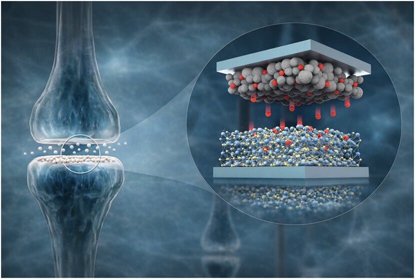
The device, developed by Senior Researcher Lee Hyun Jun and Associate Researcher Noh Hee Yeon in DGIST’s Nanotechnology Division, is an artificial synapse that uses electrically controlled hydrogen movement to simultaneously perform calculations and store results.
The research team describes this as the world’s first two-terminal AI semiconductor to achieve this using hydrogen as the active switching mechanism. The research results were published in ACS Nano.
The brain has no bottlenecks
The human brain operates on approximately 20 watts of power. It manages this by doing things that traditional computers fundamentally cannot do. That is, information is processed and stored in the same place, through the same structure, and at the same time. Synapses become stronger or weaker based on experience, and these changes themselves become memories.
Neuromorphic computing is a field dedicated to building hardware that behaves like biological neural tissue and seeks to replicate its architecture. Artificial synapses are central to this effort. This is a device whose electrical conductivity changes in response to a signal and retains that change even after the signal stops. The more closely it mimics real synapses, the more effectively the chip can learn.
Most existing approaches to building these devices rely on oxygen vacancies, defects in the material that change under an electric field and change its resistance. This method works, but comes with a permanent problem. Oxygen defects are difficult to control precisely and their behavior tends to fluctuate over time, making long-term stability a chronic challenge.
“This research has implications beyond developing another AI semiconductor,” Lee said. “This presents a new resistive switching mechanism that utilizes hydrogen transfer, which is completely different from existing oxygen vacancy-based memories.”
Hydrogen as a precision tool
The DGIST device uses a stack of thin semiconductor layers, with the active layer made of amorphous indium gallium zinc oxide, an already common material in display technology. Above that is a silicon oxide layer that acts as both a buffer and reservoir, and above that is a silicon nitride layer that acts as a hydrogen source.
Silicon nitride deposited through standard chip manufacturing processes naturally contains large amounts of mobile hydrogen, a byproduct of the gases used during manufacturing. The hydrogen becomes the working fluid for the device.
When a positive voltage is applied to the top electrode, hydrogen ions are forced through the silicon oxide layer into the active layer below. Their arrival increases the density of free electrons and increases the electrical conductivity. When the voltage is reversed, the hydrogen recedes. The silicon oxide layer controls the distance the power travels and prevents it from wandering uncontrolled when no voltage is present, which gives the device its memory.
Importantly, this switch does not occur suddenly, but gradually. The analog quality of smoothly increasing and decreasing conductance across many intermediate states allows the device to behave more like a biological synapse than a simple on/off switch. Rather than just 0 and 1, they can also represent a continuous range of values that correspond to synaptic weights (numbers that the neural network adjusts during learning).
“This is the first case in which we electrically precisely control the movement of hydrogen atoms between stacked semiconductor layers,” said Roh. “The findings from this research will fundamentally change the architecture of AI hardware and accelerate the era of next-generation low-power, high-efficiency neuromorphic semiconductors.”
Built to last and built to scale
Where promising neuromorphic devices stumble is reliability. The DGIST device exhibited no significant degradation over more than 10,000 switching cycles, held memory states stable for more than 1 million seconds of continuous testing, and had no measurable degradation in the separation between high- and low-resistance states.
The two-terminal vertical structure of this device has its own implications. A chip architecture that uses two terminals instead of three reduces cell size, simplifies manufacturing, and allows for much higher packing densities. This is critical for commercial AI hardware, as the number of synaptic connections per chip determines how complex the network will be. The structure is also fully compatible with existing CMOS semiconductor manufacturing processes, meaning that it can in principle be manufactured using infrastructure already in place across the industry.
To demonstrate that the device could actually support learning, the researchers connected the device to a simulated multilayer neural network and trained it to recognize handwritten digits using a standard benchmark dataset. The system achieved recognition accuracy of over 90 percent using only five distinct weight levels when the input images were kept at a resolution of 8 x 8 pixels or higher. This result is comparable to more complex systems that use more weight states.
This finding has practical caveats. For relatively simple tasks, the number of weight levels that a neuromorphic device can represent is a matter of less than the resolution of the input data itself. More states do not automatically improve performance.
another kind of memory
The choice of hydrogen over oxygen is not the only thing that distinguishes this approach from previous neuromorphic memory studies. It’s a physical mechanism itself. In oxygen-deficient devices, resistive switching occurs at the interface between materials due to changes in barrier height. The resulting conductance changes are inherently nonlinear, making them difficult to use as reliable synaptic weights.
In hydrogen-based devices, switching occurs throughout most of the active layer as hydrogen enters and exits. The result is a more uniform and linear change in conductance with each applied pulse, which directly translates into more predictable and controllable weight updates during neural network training.
The device also avoids one of the most stubborn failure modes in oxide-based memory. Because the hydrogen is supplied externally through the silicon nitride layer, rather than relying on pre-existing defects within the material, the source of the switching behavior is built-in and renewable, rather than relying on controlled degradation of the active layer itself.
practical meaning
The power demands of modern AI are large and increasing. To train and run large-scale neural networks, data centers need to consume as much power as a medium-sized city. Neuromorphic hardware, which processes and stores information simultaneously rather than passing data between separate components, represents one reliable path to significantly more energy-efficient AI systems.
DGIST devices are compatible with standard semiconductor manufacturing processes, lowering one of the highest barriers between laboratory demonstration and commercial production. The materials used, silicon nitride, silicon oxide, indium gallium zinc oxide, are not uncommon. The required manufacturing steps are already well understood across the industry.
Whether this particular architecture reaches production depends on further development and testing across a broader range of tasks and operating conditions. However, this study demonstrates that hydrogen movement in a vertical biterminal structure is a stable, controllable, and manufacturable basis for artificial synaptic behavior, a previously unavailable option.