
On-chip nanophotonic media configuration
On-chip optical devices can be conceptualized as systems that perform operations on a set of basic optical modes19. Similarly, on-chip analog computing systems process input information encoded in these basic modes and transform it into output modes carrying the desired information. The efficiency of this transformation, commonly referred to as coupling efficiency, directly determines the computational density of the on-chip optical computing system. As illustrated in Fig. 1a, coupling efficiency (κ), as predicted by coupled mode theory20, is influenced by refractive index perturbations within the system. Specifically, larger perturbations and greater refractive index contrasts result in higher coupling efficiencies. Consequently, enhancing these two factors is key to improving computational density in on-chip optical computing systems.
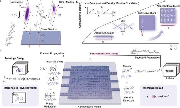
a Qualitative analysis for the coupling efficiency, which is related to the computational density in on-chip optical systems. b Comparison of different kinds of on-chip optical computational systems with computation-related coupling efficiency. c Schematic of the training and inference process of the nanophotonic media, where gradient information is calculated via the adjoint method and used to update the structures according to fabrication constraints. After fabrication, inference is achieved by light passing through the scattering nanophotonic media. Input information is encoded in the phase-modulated input light, and results are obtained through intensity detection at the output ports.
Figure 1b compares existing structures for on-chip optical computing systems with the proposed nanophotonic media, demonstrating that nanophotonic media can achieve relatively higher average efficiency. Traditional approaches, such as electrical tuning of doped waveguides, thermal tuning of waveguides, or etching diffractive structures, rely on explicit design theories. However, these methods are often constrained by empirical design principles, which limit their ability to achieve high mode coupling efficiency. In contrast, nanophotonic media enable high coupling efficiency within a compact area by overcoming the limitations of empirical design principles, thereby achieving greater computational density in on-chip systems. Nonetheless, the high coupling efficiency of nanophotonic media in such small regions also amplifies the sensitivity to fabrication-induced perturbations, which can introduce significant errors. Therefore, incorporating fabrication constraints into the design process of nanophotonic media is essential to ensure reliable system performance.
Machine learning inference in our approach is achieved using high computational density nanophotonic media, as shown in Fig. 1c, where the Iris flower classification task is taken as an example. Features are encoded into the phase modulation of waveguide eigenmodes on the left, while inference results are carried by the optical power in different output waveguides. The inference function is carried out by the nanophotonic media within the central block, where the radii of the holes in the nanophotonic media act as trainable parameters during the training process.
The training process can be viewed as solving an optimization problem under fabrication constraints and physical constraints:
$$\begin{array}{rcl}\begin{array}{c}\begin{array}{cc}{\mbox{minimize}} & {L}({{\bf{T}}}({{\bf{r}}},\,{{\bf{X}}}),\,{{\bf{t}}})\end{array}\\ \begin{array}{cc}{\mbox{subject}}\,to & g({r}_{j},{{\bf{r}}})\le 0,{{\rm{\forall }}}j\end{array}\\ \begin{array}{cc}\, & \frac{1}{{\upmu }_{0}}{{\nabla }}\times {{\nabla }}\times {{\bf{E}}}-{\omega }^{2}\varepsilon ({{\bf{r}}}){{\bf{E}}}=i\omega {{\bf{J}}}({{{\bf{x}}}}_{k}),{{\forall }}k\end{array}\end{array}\end{array}$$
(1)
where \({\mathcal L}\) is the loss function of the training process, and \({{\bf{T}}}=(\begin{array}{cccc}{{{\bf{E}}}}_{1} & {{{\bf{E}}}}_{2} & \ldots & {{{\bf{E}}}}_{n}\end{array})\) is a tensor that contains all the electric field responses with samples in the training dataset. \({{\bf{r}}}\) is the parameter to be optimized, which represents the radii of the holes in the nanophotonic media to be designed. \({{\bf{X}}}\) and \({{\bf{t}}}\) are features and labels of the training dataset. \(g\) is a function to apply fabrication constraints for each radius, and it is dynamically changed with respect to the nanophotonic media distribution. The second constraint is the physical constraint from the Maxwell Equations for the integrated optical structures with silicon and silica, where \({{{\rm{\mu }}}}_{0}\) is the permeability of vacuum, \({{\bf{E}}}\) is the electric field with the dielectric constant \(\varepsilon ({{\bf{r}}})\) and the optical source distribution \({{\bf{J}}}({{{\bf{x}}}}_{k})\) at an angular frequency of \(\omega\). The optical source distribution \({{\bf{J}}}({{{\bf{x}}}}_{k})\) is related to \({{{\bf{x}}}}_{k}\), which is the feature of a single sample in the training dataset.
We designed a gradient descent method with projection operations to solve this optimization problem. A schematic of the training process is shown in Fig. 2a. For each training sample, input sources on the left waveguides are reconfigured for simulation, and the resulting power intensities in the right waveguides are monitored and used to calculate the loss via a loss function. Gradients of the loss function with respect to the hole radii are then computed using the backpropagation method. The nanophotonic media are subsequently updated based on the gradient information and projection operations, incorporating fabrication constraints.

a Design flow of the structure parameters of the nanophotonic media with the features and label in the training dataset. b Structure parameters updating rules in each iteration. c Prediction accuracy and loss over 100 training iterations. d Confusion matrix on the test dataset. e–g The absolute value of the Poynting vector in x-direction for randomly selected inputs: e prediction of setosa; f prediction of versicolor; g prediction of virginica. h, i Comparison of designs with h no fabrication constraints and i fabrication constraints incorporated into the design process. j Comparison of the simulated fabrication variation under different fabrication tolerances with shallow etching and full etching, where vertical lines represent the 95% confidence interval.
Designing functional structures by solving optimization problems is classified as inverse design problems in integrated photonics, where ensuring the feasibility of fabricating the designed structures presents a significant challenge. An intuitive approach for ensuring fabricability involves selecting a design space that exclusively accommodates discrete, manufacturable geometries. Algorithms, such as the direct binary search (DBS) algorithm21, can be employed to explore this limited discrete design space. While this method consistently produces reliable results, it may restrict the degrees of freedom available for potential designs. Another approach for ensuring fabricability involves selecting a larger, continuous design space that includes non-fabricable geometries. Constraints are then applied within the algorithms to guide the inverse-designed structures away from these non-manufacturable geometries. Techniques like topology optimization22, shape optimization23, and methods integrated with the level-set method24 are successful and elegant for navigating continuous design spaces. In topology optimization, projection methods25 and morphological operations26 are commonly used to address non-manufacturability issues. By translating fabrication constraints into penalty terms within the optimization objectives, some methods integrated with the level-set approach have been developed to limit the minimum feature size and minimum radius of curvature27,28. Nonetheless, due to the non-convexity of inverse design problems and the discrete nature of the manufacturable design space, incorporating efficient fabrication constraints into inverse design methods remains a significant challenge.
In our approach, the design space is discretized into nano-block arrays while maintaining the radius of the hole structures within each block as continuously tunable, thereby achieving a large design parameter space. At the same time, we specify dynamically changing constraint rules to ensure that all hole structures meet fabrication constraints. After calculating the gradient information using the adjoint method23 in each iteration, we apply a projection operation based on the gradient information and the current structural state to optimize all structures under fabrication constraints until the iteration limit is reached (details and comparison with the topology optimization are described in Supplementary Note 1), as shown in Fig. 2b. The gradient information is obtained using samples and labels from the task dataset, enabling a training process for the structure to learn and adapt to the target task.
We use the Iris flower dataset to train and test the nanophotonic media. This dataset consists of 150 data points18 for classifying three types of Iris flowers: setosa, versicolor, and virginica. Each of the data points has four flower features. These features are normalized and rescaled to fit within the 0-π phase range of the eigenmode sources of the input waveguides. The nanophotonic media system is trained using 80% of the dataset, with the remaining 20% reserved for testing the trained system. The nanophotonic media that works as an Iris flower classification inference function is an 8×8 µm2 region in the center with 20 × 20 70 nm shallow etched holes, which is shown in Fig. 1c. Diameters of these holes vary from 130 to 400 nm, ensuring the fabricability. As part of the SOI platform, the 220 nm thick silicon material is on top of a 2 µm silicon oxide box and covered by 1 µm silicon oxide. Diameters of the holes are learned from the Iris flower dataset. After fabrication, the nanophotonic media can identify the category of an Iris flower with unlearned features.
A normalized mean square error (NMSE) loss function (details in Supplementary Note 2) and a batch gradient descent strategy using the adaptive moment estimation (Adam) optimization algorithm are employed for the training process. Figure 2c and Fig. 2d illustrate the evolution of the NMSE loss, prediction accuracy in the training process, and the confusion matrix on the test dataset after training, respectively. An accuracy of 86.7% is achieved on the test dataset after 95 training iterations. Figure 2e–g display the absolute value of the Poynting vector in the x-direction for randomly selected inputs corresponding to the three types of Iris flowers.
After training, the nanophotonic media are capable of processing machine learning tasks with computation performed through scattering blocks composed of numerous holes within the media. The minimum feature size for the etching process is 130 nm. A comparison of the design without fabrication constraints is shown in Fig. 2h and Fig. 2i, where the proposed fabrication constraints not only eliminate excessively small patterns but also facilitate passing the design rule check (DRC) for commercial lithography (details in Supplementary Note 3). Besides designing for fabrication rule compliance and ensuring fabrication performance, we also significantly enhance the fabrication tolerance of our design by adopting a low-index-contrast approach. A comparison of simulated fabrication variations across different tolerance levels is shown in Fig. 2j. Fabrication tolerances were analyzed using the Monte Carlo method (see Supplementary Note 4 for details). Although full etching with high index contrast has a stronger influence on the field distribution within the same design region, when the design region is sufficiently large, both shallow-etch and full-etch approaches can provide adequate functional structures. Our results indicate that employing shallow etching with low index contrast effectively reduces the impact of fabrication variations. While the original full-etch design exhibits substantial performance degradation at 20 nm process variations and becomes nearly non-functional at 50 nm variations, the shallow-etch design maintains satisfactory performance even under 50 nm variations. It is worth noting that the 20 nm tolerance value, which serves as the starting point in Fig. 2j, already represents a conservative estimate, as it exceeds the typical requirements of most real-world fabrication processes.
Experiment
The experimental setup with the fabricated chip is shown in Fig. 3a. The chip is fabricated using electron-beam lithography at the Center for Advanced Electronic Materials and Devices (AEMD) of Shanghai Jiao Tong University. Optical microscope and scanning electron microscope images of the nanophotonic media region are shown in Fig. 3b and c, respectively. The input light with a wavelength of 1550 nm is coupled into the chip through a single grating coupler and then split by three power splitters to generate four coherent light sources for the nanophotonic media. Four phase modulators are integrated on the waveguides of these four coherent light sources, each capable of providing a phase shift from 0 to π with different voltages. To minimize additional phase difference errors, the lengths of the four input waveguides are designed to be equal. At the output of the nanophotonic media, three waveguides and three couplers are used to direct the light carrying the results to output fibers, where it can be detected by off-chip photodetectors. Both simulation and measurement results consistently show an insertion loss of approximately 10 dB, which could potentially be improved by incorporating transmission-enhancing terms into the loss function during the device design optimization process (see Supplementary Note 5 for details).

a Experiment setup for the fabricated chip. b Microphotograph of fabricated chip and c Scanning electron microscope photo for the nanophotonic media. d Confusion matrix on the test dataset after compensation. e Experimental normalized intensity distributions for all the samples in the test dataset after compensation. The ground truth labels for sample indices 0–9 are setosa, for 10–19 are versicolor, and for 20–29 are virginica. f Comparison of size and latency for on-chip inference systems4,5,7,11,12,13. Latency in this work is calculated in Supplementary Note 9. Lines indicate achievable latency ranges through component refinement. HandWritten-n represents the n-category handwritten digits dataset. *Area estimated from microscope images. †Latency obtained through theoretical calculations.
After performing a phase to on-chip phase conversion (details are described in Supplementary Note 6), we map the input features to the voltages required for the phase shifters. For each test sample in the dataset, we apply the corresponding voltages to the phase shifters and measure the light power intensities of the three outputs, which represent the probability of the predicted category. We applied a compensation procedure to mitigate fabrication imperfections and inconsistencies in the grating couplers (details are described in Supplementary Note 7). Before applying this compensation, the experimental test accuracy was 50.0%. After compensation, the accuracy was improved to 86.7%. The confusion matrix after compensation is shown in Fig. 3d (the one before compensation is shown in Supplementary Note 7). Experimental normalized intensity distributions for all the samples in the test dataset are shown in Fig. 3e. The experimental inference results are consistent with the designed inference outcomes (simulated normalized intensity distributions are shown in Supplementary Note 7). The broadband capability of the design extends up to 100 GHz, characterized by evaluating frequency shifts of ±50 and ±100 GHz, which correspond to practical modulation scenarios (see Supplementary Note 8 for details).
Figure 3f illustrates the comparison of size and latency for on-chip inference systems. The scattering process in this work efficiently mixes and modulates the input light over a short distance, leading to a reduction of more than three orders of magnitude in size for on-chip machine learning inference platforms. This miniaturization also translates to a shorter propagation distance, thereby reducing system latency (latency calculations are provided in Supplementary Note 9). However, compared to the latency introduced by the input section of the system, the latency in the computational block is significantly lower. As a result, Fig. 3f does not fully reflect the advantage of reduced computational latency. To address this, we calculate the latency of the computational block separately and discuss it further in the Discussion section.
Hand written digit images Recognition
To further validate the performance of the proposed nanophotonic media for machine learning inference, a larger region with 64 input waveguides is trained to recognize handwritten digit images for optical character recognition (OCR) systems. The open-source dataset29 comprises 3823 training images and 1797 test images. The 8 × 8 pixels of the images are directly encoded into the mode phase of 64 input waveguides. The nanophotonic media for the OCR as shown in Fig. 4a consist of a 112 × 112 array of holes within a 44.8 × 44.8 µm2 area. NMSE loss and Adam optimization algorithm are adapted for the training process, and a batch gradient descent strategy is employed. Similar to the Iris flower classification task, we employed a low-index-contrast design with a minimum feature size of 130 nm.

a Schematic of hand written digit images recognition inference. The inset in a shows sample images of digits ‘0’, ‘3’, and ‘9’. b Confusion matrix on the test dataset. c Prediction accuracy and loss over 50 training iterations. The sample images shown in the inset of a are visualizations of data derived from the Optical Recognition of Handwritten Digits dataset29, in accordance with the Creative Commons Attribution 4.0 International License (CC BY 4.0; https://creativecommons.org/licenses/by/4.0/).
After training, the inference accuracy on the test dataset is 92.8%. Figure 4b displays the confusion matrix on the test dataset after training. Figure 4c shows the evolution of the prediction accuracy and NMSE loss in the training process. The final structure is shown in Supplementary Note 10. The results demonstrate that nanophotonic media have the potential to process large-scale tasks within a very small area, significantly enhancing space efficiency for on-chip optical computations.
Fabrication tolerances were analyzed using the Monte Carlo method (see Supplementary Note 11 for details). In the scaled design, employing low-index-contrast structures effectively reduces the impact of fabrication variations. The tolerance-enhanced device achieves an average test accuracy of 89.7% under a 20 nm fabrication tolerance—well within practical fabrication limits—and maintains 53.6% accuracy even with a 50 nm tolerance. Furthermore, post-fabrication compensation strategies can further mitigate the influence of fabrication errors as well as input noises and output noises (see Supplementary Note 12). The broadband performance was also characterized by evaluating frequency shifts of ±50 and ±100 GHz, corresponding to practical modulation scenarios (see Supplementary Note 13). Across all tested frequency shifts, the test accuracy remained above 91%. Temperature sensitivity was also investigated through simulations, showing that the device maintains a test accuracy of 86.9% under a 40 K temperature variation (see Supplementary Note 14).


