Workflow fitted for the NEP model
As illustrated in Fig. 1, an active learning workflow was employed to develop a high-accuracy MLP for carbon deposition. This framework iteratively integrates NEP training and DFT validation during hybrid MD/tfMC simulations of a-C film growth on a Si(111) surface. To describe carbon–carbon interactions, we adopted the publicly available GAP-20 dataset introduced by Rowe et al. as the initial training dataset43. This dataset, consisting of 6082 diverse carbon structures, serves as the starting point for our active learning loop. We first retrained the GAP-20 dataset using the NEP framework to generate a reference model, denoted as NEP-20, and the training results are shown in Fig. S1. To reduce redundancy and improve data efficiency, we applied a farthest-point sampling strategy44 using the pynep toolkit to streamline the dataset. As shown in Fig. S2a, this reduced the number of structures from 6082 to 3681. The resulting streamlined dataset was used to train a more efficient potential, SNEP (training results are shown in Fig. S3). Its accuracy was benchmarked against DFT using the radial distribution function (RDF), phonon dispersion, energy–volume (E–V) curves, and lattice constants of representative carbon phases (Fig. S2b–d and Table S1). These results confirm that the filtering process does not compromise model fidelity. This streamlined dataset, in combination with additional configurations for pure silicon and interfacial C–Si systems (see Table S2), was then used as the starting point for the subsequent active learning loop. Detailed information on all datasets can be found in Table S2.
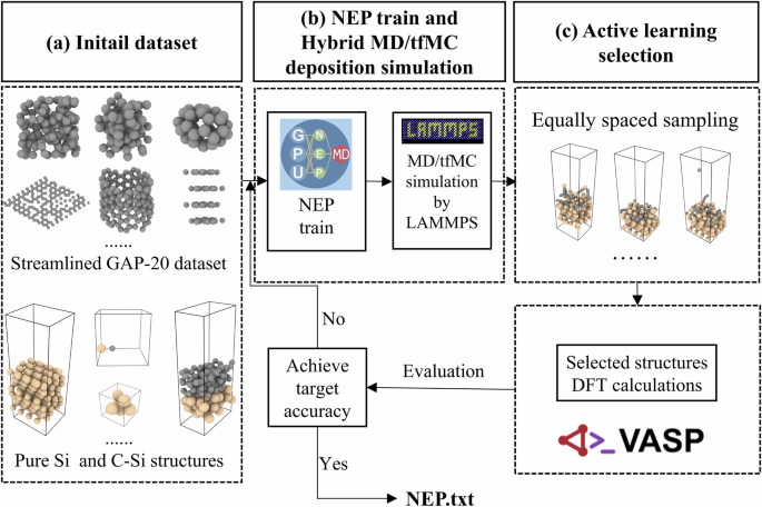
a The initial training dataset consists of the streamlined carbon GAP-20 dataset43, pure Si, and C-Si interaction datasets. Detailed information on all datasets can be found in Table S2. b The NEP obtained after training on the dataset is subjected to coupled MD/tfMC simulations. c The simulation-derived trajectories are sampled isometrically and the static calculation of the DFT is performed. Subsequently, the sampling structure is evaluated to see if it achieves accuracy, and if the structure is larger than the threshold of the error for the current round then the structure is added to the training set to continue training, otherwise the iteration is completed and the potential file is output. The black and khaki spheres represent carbon and Si atoms, respectively.
Once the initial NEP was trained, it was coupled with LAMMPS to perform MD/tfMC of carbon atom deposition under multiple target energetic conditions. This hybrid simulation approach enabled the efficient exploration of atomic configurations and facilitated the formation of metastable amorphous or graphitic-like domains on the substrate surface, mimicking experimental deposition environments with different incident energies. The trajectories generated from the MD/tfMC simulation are sampled in equal spacing, and subsequently the Vienna Ab initio Simulation Package (VASP) software is applied to the sampled structures in each round to perform DFT calculations, and we use the NEP of the current round to predict the sampled structures to obtain the RMSE-pre. Subsequently, all the sampled structures are added to the training set, and in the same MD/tfMC simulation, then the structures are sampled and predicted to get the RMSE-post, if the two RMSEs are the same, we consider that the NEP reaches the target accuracy. The loop was repeated until the model converged to a predefined accuracy threshold.
Composition of the dataset
Based on the fitting workflow described above, a total of 5116 structures were obtained during the final training iteration. To assess the structural diversity and energy landscape of the curated the dataset, we projected it into a low-dimensional space using sketch-map, as shown in Fig. 2. Each structure is represented by a colored point, with its position indicating similarity in learned descriptors derived from principal component analysis (PCA)45 and its color encoding the average atomic energy. The sketch-map reveals a well-structured yet complex distribution, with two primary branches corresponding to pure carbon and Si-rich environments. The left region is densely populated with carbon-only configurations, ranging from sp3-like amorphous clusters to sp2 graphene-like sheets and linear chains. Representative structures confirm these motifs, highlighting the NEP model’s comprehensive coverage of carbon bonding environments. In contrast, the right region is dominated by Si-rich structures, including crystalline Si lattices, surface slabs, and mixed C–Si interfacial configurations. A smooth gradient in atomic energy across the manifold suggests that the dataset captures a continuous interpolation from high-energy nonequilibrium configurations to low-energy stable ones, a desirable feature for robust force-field training46. Notably, the transition region between the carbon and Si branches contains hybrid structures with diverse local coordination environments, which are critical for accurately capturing interfacial interactions during the early stages of carbon film nucleation.
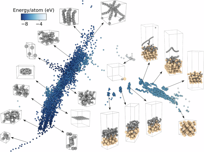
Each dot’s position is obtained via PCA of the learned descriptors, with color representing the corresponding atomic energy. The black and khaki spheres represent carbon and Si atoms, respectively.
Training results for the dataset
The final training results for the dataset are presented in Fig. 3, illustrating the generation-wise evolution of the loss function during NEP training. The total loss, L1 and L2 regularization, as well as the energy, force, and virial loss functions, converge after about 200,000 generations (Fig. 3a). Figure 3b–d shows that the RMSE of convergence for energy, force, and virial for the training dataset are 56.892 meV/atom, 552.347 meV/Å, and 140.507 meV/atom, respectively. For the test dataset, the RMSE of convergence were 57.752 meV/atom, 555.817 meV/Å, and 146.567 meV/atom for energy, force, and virial, respectively. It is worth noting that the error value of the fit is slightly larger than some MLPs for crystals due to the rich carbon structure contained in the dataset as well as the structural complexity of the depositional growth, but this fit is comparable to or even lower than the results of other GAP-20 carbon-based MLPs training47,48. This indicates the effectiveness of the training method as well as a computational accuracy close to that of DFT. At the same time, the wide range of energy, force, and virial in the training dataset ensures the stability of the NEP-based MD in various deposition scenarios.
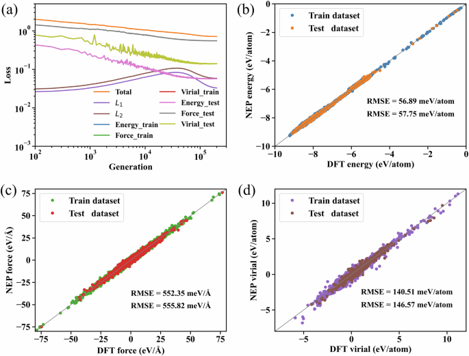
a Evolution of the various terms in the loss function for the training and testing datasets with respect to the generation. b Energy, c force, and d virial calculated as compared to the DFT reference data for the training and testing datasets.
Results of carbon growth on Si(111) substrates
By employing a highly accurate NEP and incorporating rare atomic events via the hybrid MD/tfMC approach, we successfully reproduce the carbon growth process on Si(111) substrates, the results are shown in Fig. 4. The growth results following the completion of carbon deposition are visualized in Fig. 4a. The Si(111) substrate is color-coded based on height, while carbon atoms are rendered in blue. Two distinct types of structures can be identified from the results. The first type observed at low incident energies (5–20 eV) consists of disordered graphene network (DGN)49 of loosely connected. This structure exhibits three-dimensional connectivity and a relatively high degree of graphitization, and is often referred to as porous carbon50, pyrolytic carbon51, or amorphous graphite49. Such DGNs can also be obtained by quenching under low-density conditions48. Previous studies have shown that this structure is characterized by negative-curvature microstructures52, comprising saddle-shaped graphene nanosheets with out-of-plane topological defects53. Structurally, the DGNs exhibit short-range order but long-range disorder, which originates from the randomly oriented graphene nanosheets. In contrast, at higher incident energies (50–100 eV), the resulting structure is an a-C phase with a higher degree of disorder. Notably, under high-energy impacts, Si atoms from the substrate become increasingly incorporated into the carbon film as the incident energy rises. For the same number of deposited atoms, the film thickness resulting from low-energy deposition is significantly greater than that formed at high energies, indicating a marked difference in atomic density. This is further evidenced by Fig. S4, which shows the variation in atomic density along the Z-axis of the simulation box. In the region above the substrate, the atomic density under 5–20 eV is significantly lower than that observed under 50–100 eV. These results demonstrate a clear dependence of the resulting film structure on the incident energy, highlighting the energy-dependent nature of the carbon growth process.
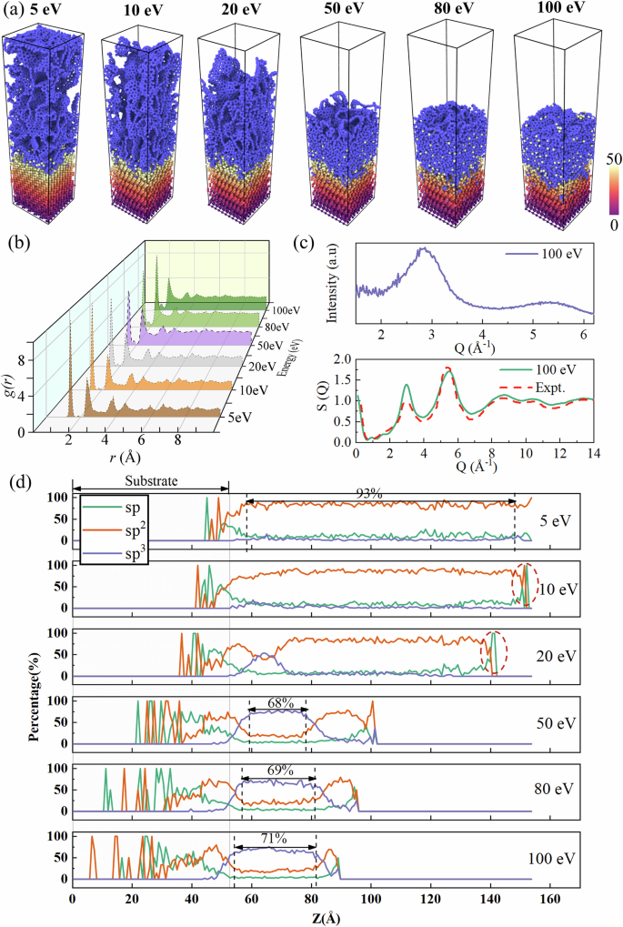
a Visualization of the end of carbon deposition. Si(111) substrates are color-coded by height and carbon atoms are shown in blue. b RDF of different energies. c XRD spectral curves and structure factors for carbon films obtained at 100 eV. The experimental data of the structural factors were obtained from the work of Gilkes et al.55. d Distribution of carbon atoms with sp, sp2, and sp3 hybridizations as a function of Z-axis.
The RDF characterizes the probability of finding other atoms in a spherical shell centered on any atom, and the overall characteristics of the system can be understood based on the shape and location of the peaks54, as shown in Fig. 4b. The main peak at 1.47 Å (corresponding to the typical C-C bond length)21, decreases with increasing deposition energy, indicating that high-energy conditions hinder the formation of sp2-hybridized DGNs. Multiple oscillatory peaks suggest short-range order without long-range periodicity. We calculated the X-ray diffraction (XRD) pattern and structure factor of the a-C film formed at an incident energy of 100 eV, as shown in Fig. 4c. The XRD profile closely resembles that of annealed amorphous diamond reported by Zhu et al.49. Additionally, the computed structure factor is in good agreement with that of tetrahedral amorphous carbon (ta-C) presented by Gilkes et al.55. These results indicate that high-energy deposition indeed leads to the formation of a tetrahedrally coordinated DLC film, further confirming the reliability of the potential in accurately modeling the deposition process.
Subsequently, we counted the distribution of sp, sp2, and sp3 hybridization of carbon atoms in the system as shown in Fig. 4d. Hybridization types are determined based on the number of neighboring atoms within a cutoff distance of 1.85 Å—2, 3, and 4 neighbors corresponding to sp, sp2, and sp3, respectively. At low energies (5–20 eV), the sp2 structure dominates throughout the film, consistent with the formation of DGNs. Notably, a significant increase in sp hybridization is observed near the end of the growth direction (highlighted by dashed ellipses) at 10 and 20 eV. This feature is absent at 5 eV, possibly due to limitations in the simulation box height, which prevent the complete capture of structures near the growth front. As shown in Fig. S5, when only 7000 carbon atoms are deposited at 5 eV, sp-hybridized carbon atoms (i.e., carbon chains) also appear at the growth front, consistent with the results observed at 10 and 20 eV. These results suggest that at low energies, film growth initially proceeds through sp-hybridized carbon chains, which gradually transition into sp2-bonded structures as accumulation progresses. The sp2 content in our simulations reaches approximately 93%, closely aligning with the 97% sp2 fraction previously reported in DGNs by EELS measurements56. With increasing deposition energy, a distinct transition toward sp3 bonding is observed in the central region of the carbon film, particularly at 50 eV and above. At 50, 80, and 100 eV, the local sp3 fractions reach 68%, 69%, and 71%, respectively, indicating the formation of DLC films. Our simulation results are consistent with those of Y. Lifshitz who used mass-selected ion beam source to deposit carbon films on Si substrates57. Their atomic force microscopy studies showed that when the C+ ion energy exceeded 30 eV, the resulting films exhibited DLC structures, whereas graphite-like films formed at energies below 30 eV.
This finding is unattainable using the extensive empirical potential like Tersoff58, as shown in Fig. S6. We performed carbon deposition simulations using the Tersoff potential under the same parameter settings as those used for the NEP model, including incident energies of 5, 10, 20, 50, 80, and 100 eV, all at a temperature of 300 K. The simulation results obtained with the Tersoff potential differ significantly from those of the NEP model at both low and high energies, as shown in Fig. S6a. Complex DGNs are not formed at low energies, nor are compact atomic structures formed at high energies. Figure S6b shows the type of bonding of carbon atoms with respect to the Z-axis. It can be seen that at either energy, the carbon atoms are bonded as sp2 bonds and sp3 bonds are rare. This is clearly not in accordance with the experimental observation59. Moreover, deposition simulations based on the widely used EDIP potential also fail to produce a-C structures with an sp3 fraction exceeding 60%60. Therefore, we believe that the simulation achieves a level of accuracy comparable to experimental results, despite minor discrepancies introduced by differences in temporal and spatial scales.
Process analysis of carbon growth on Si(111) substrates
We further evaluated the accuracy of the fitted NEP in characterizing the carbon growth process using 5 eV and 50 eV energies as examples. Figure 5a, b depict the time evolution of carbon atoms with different coordination numbers during deposition, ranging from C0 to C5, where CN denotes carbon atoms with N nearest carbon neighbors. At 5 eV, the number of C2 increases slowly, whereas the number of C3 increases rapidly and dominates throughout the simulation, suggesting that it is the sp2-bonded carbon atoms, represented by graphene-like, that are predominantly generated. In contrast, a more complex behavior is exhibited at 50 eV, with C2 growing rapidly at the beginning of the growth period starting to decline and leveling off at 25 ns, and the ratio of C3 and C4 coordination atoms increasing significantly with time, however, the number of C4 exceeds that of C3 at about 55 ns, reflecting a shift to a sp3-like overcoordinated environment due to high-energy injection and local structural rearrangements, which is in agreement with the observation in Fig. 3a. Notably, at all examined energy levels, carbon atoms exhibit a sequential evolution from C0 to C4 (i.e., C0 → C1 → C2 → C3 → C4), as evidenced by the embedded diagrams in Figs. 5a, b as well as the growth results at other energies shown in Fig. S7.
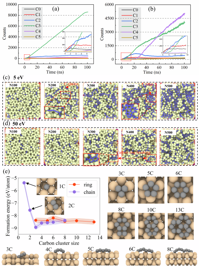
a, b Illustrate the temporal evolution of carbon atoms with different coordination numbers during the simulation at 5 eV and 50 eV, respectively, where C0 to C5 represent carbon atoms with 0 to 5 nearest neighbors. Here, we remove the time consumed by relaxation and tfMC. c, d Show top-view snapshots of the deposition process following the deposition of carbon atoms at 5 eV and 50 eV, respectively, highlighting the formation and structural evolution of carbon chains and rings, where X in NX denotes the number of carbon atoms. e The formation energies of various carbon chains and rings composed of different numbers of carbon atoms by DFT calculations; the right subpanel shows the relaxed structures of carbon rings with varying atomic configurations, while the lower subpanel displays corresponding carbon chain structures.
Figure 5c, d show atomic snapshots of the top surface region with different numbers of carbon atoms at 5 eV and 50 eV, respectively. The NX on the upper left corner represent the corresponding X atoms deposited onto the substrate. When a small number of carbon atoms are deposited onto the substrate they mainly exist as monomers or dimers corresponding to C0 and C1 respectively (N100). At 5 eV, we begin to observe the formation of linear carbon chains, with some extending to more than eight atoms (N200), this feature is absent at 50 eV. The carbon atoms tend to stay on the surface and grow along it, whereas at higher energies, they are more likely to embed into the substrate, as shown shadows of the substrate in Fig. 4d. Moreover, carbon atoms arriving at high energy often collide with the structures formed earlier, breaking up existing chains. This can be clearly seen in the snapshots from N300 to N400 at 50 eV, where two six-membered rings are disrupted by incoming atoms, resulting in the formation of shorter fragments. In contrast, the same stage at 5 eV (N300–N400) shows more complete six-membered rings and longer chains, forming graphene nanosheets.
We used DFT calculations to compare the energetic preference of carbon ring and chain structures composed of different numbers of carbon atoms on the Si(111) surface, as shown in Fig. 5e. For the ring structures, we selected compact configurations that were observed in our simulations. The results reveal a sharp energy drop up to the formation of 3-membered carbon clusters, after which the energy difference between ring and chain configurations with the same number of atoms becomes relatively small. This energetic proximity explains the coexistence of carbon rings and chains during the growth process. Notably, this behavior contrasts sharply with the findings of Van Wesep et al. for carbon structures on Cu(111)61, where all linear configurations were found to be energetically more favorable than their ring counterparts. Compared to Cu(111), the Si(111) surface exhibits moderate binding strength with carbon atoms—sufficient to partially compensate for the bending strain associated with divalent carbon atoms in ring structures62. Consequently, C–Si interactions can partially passivate the dangling σ bonds at the bent vertices of carbon rings, stabilizing them to a degree not possible on Cu surfaces, while still preserving the possibility of chain formation. These results fully demonstrate the ability of NEP in capturing the formation and evolution of carbon chains and rings on the Si(111) surface, which has never been seen in previous studies.
Mechanistic analysis of carbon film growth on Si(111) substrates
This difference in growth results due to the incident energy of carbon atoms prompts us to think about what exactly is the energy-dependent growth mechanism of carbon films. To evaluate the performance of the NEP in characterizing the dynamics and growth mechanisms of a-C films, we employed a two-dimensional cylindrical projection method to analyze atomic-scale changes in density and bonding during the deposition process. This method calculates the local mass density difference, denoted as Δρ = (r, h), which captures the redistribution of carbon atoms in the radial-axial plane centered at the impact point of each deposited atom. The formalism is given by refs. 14,30:
$$\Delta \rho (r,h)=2\pi r[{g}_{\mathrm{after}}(r,h)-{g}_{\mathrm{before}}(r,h)]$$
(1)
where r is the radial distance from the incident trajectory (impact axis), and h is the vertical height relative to the impact point. \({g}_{before}(r,h)\) and \({g}_{{\rm{after}}}(r,h)\) represent the RDF of the initial point of carbon atoms at the moment of arrival at the surface of the film and the residence position of the atoms at the end of deposition, respectively. This differential density map reflects local accumulation (positive ∆ρ) or depletion (negative ∆ρ) of atoms, and can be further decomposed by bonding types—such as sp2 and sp3 to trace local hybridization dynamics.
Figure 6a presents heat maps of the local density variation during carbon atom deposition under various incident energies, including total mass density, as well as sp2 and sp3 hybridized components. In each subplot, the coordinate (0, 0) represents the deposition site of the incoming atom, marked by a pentagram. Each image is obtained by averaging over 4000 deposition events. The spatial variation of density is shown as a function of radial distance r and vertical height h. At 5–20 eV, the changes in total mass density are mostly confined to the immediate vicinity of the impact site, indicating that carbon atoms tend to adsorb directly onto the surface. In this regime, rebonding processes are strongly influenced by thermal fluctuations, resulting in a more random spatial distribution, and the formation of sp3 bonds is minimal. As the deposition energy increases to 50 eV and beyond—entering the regime associated with DLC formation—the sp2 component remains concentrated near the impact site, whereas the sp3 component exhibits a distinct lateral expansion away from the center. This suggests that higher energies facilitate the formation of fourfold coordination bonds within the film interior. Notably, at high energies (80 and 100 eV), a local dissipation in sp3 density emerges near the impact cylinder (approximately 4 Å in width and 10 Å in depth), accompanied by a significant increase in atom density in the surrounding 5–10 Å region. This observation contradicts the traditional subplantation model63,64, which is the general consensus for carbon film growth. Instead, it supports a high-energy impact induced lateral reconstruction mechanism where sp3-rich structures preferentially form around rather than within the impact zone. This phenomenon is known as the “penning” growth mechanism60,64. However, although the “peening” growth mechanism was demonstrated on a-C substrates by Caro et al.14. We have extended this finding to Si (111) substrates using an accurate NEP model. This is important because in engineering applications a-C films are often grown on different materials to be used as protective coatings2,65. Although current experiments and DFT calculations cannot yet confirm the peening growth mechanism, this novel prediction based on the high-fidelity NEP model awaits further validation from both theoretical and experimental studies.
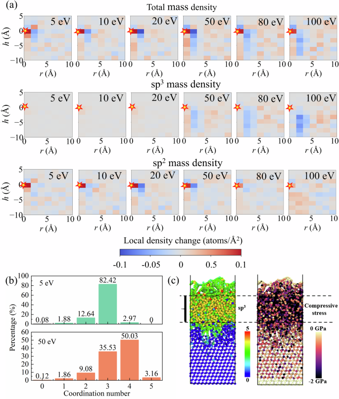
a Presents heat maps of mass density variations for all atoms (top row), sp2-hybridized atoms (middle row), and sp3-hybridized atoms (bottom row), respectively. The pentagram at the coordinate origin (0, 0) indicates the position of surface impact. Density variations are averaged over 4000 deposition events, with the color gradient from red to blue indicating regions of increased to decreased local density. b Shows the statistical distribution of atoms with different coordination numbers averaged over 4000 deposition events, while c depicts the atomic structure at 50 eV, colored by coordination number and stress, respectively.
We are counting the average change in the coordination number of carbon atoms in the system due to the process of 4000 deposition events, as shown in Fig. 6b. At 5 eV, the population is overwhelmingly dominated by 3-fold coordinated (sp2) carbon atoms (82.42%), with only 2.97% forming 4-fold (sp3) configurations. This distribution aligns with the observed density accumulation pattern and confirms the predominance of DGNs. Upon increasing the deposition energy to 50 eV, however, the sp3 fraction rises sharply to 50.03%, while sp2 atoms account for 35.53%. The concurrent increase in 4-fold coordination and sp3 density in the maps reflects a clear energy-induced bonding transition from planar to tetrahedral motifs. These transformations are further visualized in Fig. 6c, which displays atomistic snapshots colored by coordination number (left) and local stress (right) under 50 eV conditions. sp3 atoms cluster beneath the surface, forming a connected high-density phase embedded in a more disordered matrix. The stress map reveals that this sp3-rich region coincides with zones of elevated compressive stress. Such compressive states are a direct result of atom crowding and volume collapse under high-energy impact, which thermodynamically favors tetrahedral configurations21. This correlation between stress localization and hybridization supports a mechanochemical coupling mechanism, wherein stress fields mediate bonding transitions during growth66.
Transferability of NEP fitting workflows
The above results highlight the efficiency of the NEP in simulating the growth of a-C films. To evaluate the transferability of the NEP model, we extended the training within an active learning framework to include the growth of carbon on Cu(111) and Al2O3(0001) substrates. Based on the energy selection from previous simulation studies10,67, the growth of carbon on both substrates was carried out at 1 eV. The simulation results are shown in Fig. 7. It is noteworthy that two substrates represent the prototypical metal and oxide substrates that have been widely used in experimental studies of the synthesis of carbon-based nanostructures11,13,68. Figure 7a shows a top view of the carbon morphology formed on the Cu(111) surface at different deposition stages. The evolution of the carbon morphology goes through three distinct stages as the carbon coverage increases from 10 to 500 atoms: (i) early diffusion of carbon monomers below the subsurface and migration of carbon atoms to form C dimer (N10), (ii) formation of isolated linear carbon chains (N100), and (iii) nucleation and coalescence of the carbon ring into an extended sp3 network (N200–N500).
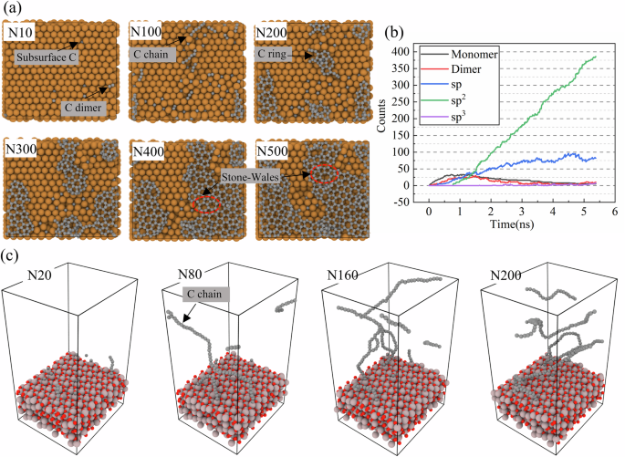
The NX on the upper left corner represent the corresponding X atoms. a Different numbers of carbon atoms deposited on Cu(111) substrate, with carbon in gray and copper atoms in yellow. b Carbon deposited on the Cu(111) substrate during the growth process. c Different numbers of carbon atoms deposited on an Al2O3(0001) substrate, with carbon in gray, Al in pink, and O in red respectively.
In addition to the standard six-membered ring, Stone–Wales (SW)-like defects with numerous five- and seven-membered rings are formed (dashed circles). SW defects represent a typical form of topological reconstruction, commonly formed in two-dimensional materials as a result of stress accumulation. Their emergence is often closely related to stress-relief mechanisms, particularly in heteroepitaxial systems, where lattice mismatch at the interface induces local strain that can be alleviated through the formation of SW defects. This mechanism of strain accommodation via defect formation has been widely reported in the growth of materials such as phosphorene69, silicene70, and graphene71. The quantitative evolution of different carbon bonding configurations is shown in Fig. 7b, which tracks the number of monomers, dimers, and sp, sp2, and sp3 hybridized atoms over time. The number of sp2-hybridized atoms steadily increases and eventually dominates, while sp-hybridized atoms remain relatively scarce. The copper substrate facilitates surface diffusion and rehybridization of carbon, resulting in the formation of ordered graphene domains. This growth behavior is consistent with experimental reports identifying copper as an effective catalytic surface for 2D carbon crystallization and is further supported by recent work from Zhang et al. who used a MLP based GAP model to simulate carbon growth on metal substrates10.
In contrast, deposition on Al2O3 (0001) substrates yields significantly different structural features, as shown in Fig. 7c. Instead of forming compact ring or sheet structures, the carbon atoms are assembled mainly into disordered, vertically extended chain-like structures with very limited lateral connectivity. As the carbon coverage increases from N20 to N200, the deposited atoms form branched flexible filaments rather than coalescing into two-dimensional films. Although direct experimental evidence of carbon chains on Al2O3 substrates is rare, their existence has been confirmed in other systems. In 1972, Baker et al. observed carbon chains formed during nickel-catalyzed carbon deposition via TEM72, and later studies have imaged atomic-scale carbon chains synthesized by mechanical methods73. DFT calculations by Zhao et al. showed that methane dissociation on γ-Al2O3 yields CH2 intermediates that couple into vertically growing carbon chains due to weak substrate interactions74. To support this mechanism, we performed AIMD simulations by randomly placing 200 carbon atoms on an Al2O3(0001) surface and relaxing the system at 300 K. As shown in Fig. S8, vertically oriented disordered carbon chains formed after 2320 fs (Fig. S8a), and the system energy stabilized (Fig. S8b), indicating thermodynamic stability.
Graphene growth on Al2O3 is challenging due to the substrate’s weak catalytic activity and the high energy barriers that impede the formation of carbon rings, ultimately hindering the development of extended sp2 networks10,75. It is worth noting that the experimental preparation of high-quality graphene films often requires high-temperature conditions, and we only considered room temperature at 300 K in our simulations, which should improve the quality of graphene if the simulation temperature is raised. However, the quality of graphene grown on insulating oxide substrates will still be lower than on metal catalysts68,75,76. These simulations reveal a pronounced substrate effect during the early stages of carbon film nucleation and growth. The results confirm the robustness and transferability of the NEP training framework and further demonstrate its capability to capture substrate-dependent growth pathways at the atomic level, providing valuable guidance for the selection of optimal substrates in the fabrication of carbon-based nanostructures.


