June 5, 2026
news
Ayar Labs joins the NVIDIA NVLink Fusion ecosystem by making its solutions optically and electrically compatible with NVIDIA’s optical and SerDes technologies, enabling hyperscalers and system designers to build optically connected AI infrastructures around NVIDIA’s NVLink Fusion platform and partner ecosystem.
“AI infrastructure is co-engineered from the ground up, and as bandwidth continues to increase, customers need more options to efficiently scale performance,” said Mark Wade, CEO of Ayar Labs. “By joining the NVIDIA NVLink Fusion ecosystem, we are introducing co-packaged optics as a foundational building block for customers deploying heterogeneous computing in the NVIDIA AI Factory.”
Ayar Labs’ CPO is designed to address scaling limitations by bringing high-bandwidth, low-latency, power-efficient connectivity to the NVLink Fusion architecture. This facilitates customers who want more design headroom as their bandwidth requirements grow and electrical constraints increase.
This collaboration allows users to maintain their investment in NVLink-based architectures while helping them deploy heterogeneous computing, including custom silicon, within the NVIDIA rackscale platform. According to a press release, NVLink Fusion provides a gateway for integrating custom CPUs and XPUs into NVIDIA’s rack-scale architecture and ecosystem.
“NVLink Fusion combined with Ayar Labs’ CPO technology gives customers more options for building heterogeneous AI factories,” said Ashish Karandikar, Vice President, NVIDIA. “Expanding the NVLink Fusion ecosystem with Ayar Labs optical connectivity will enable innovators to scale bandwidth and bring heterogeneous AI infrastructure to market faster.”
Ayar Labs works with clients to coordinate the integration of CPO and NVLink Fusion deployments, including system architecture, validation requirements, and platform timelines.
For more information, please visit www.ayarlabs.com.
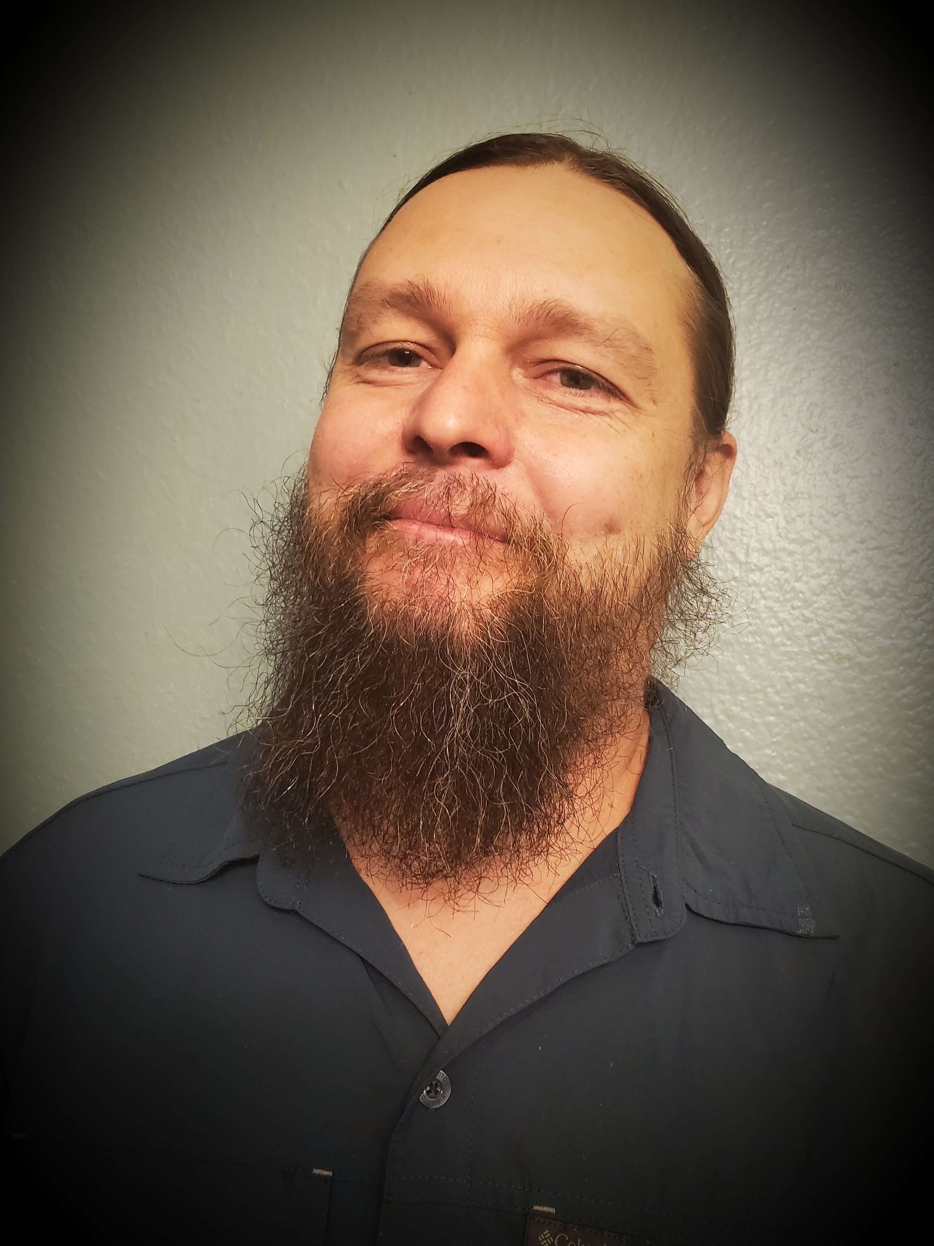
Chad Cox is a production editor at Embedded Computing Design. His responsibilities center around content creation, writing and editing, and article research and development. Chad is known for covering industry news and events and interacting with various industry leaders through on-premises visits and online interviews. He is responsible for distributing news through our digital footprint and social media posts, creating advertising, and producing newsletters. Embedded Computing Design Daily.
He is well-versed in various aspects of industrial computing including edge AI, IoT, processing, security, open source, and more.
Chad graduated from the University of Cincinnati with a bachelor’s degree in cultural analysis literature and a master’s degree in education.
Other works by Chad