
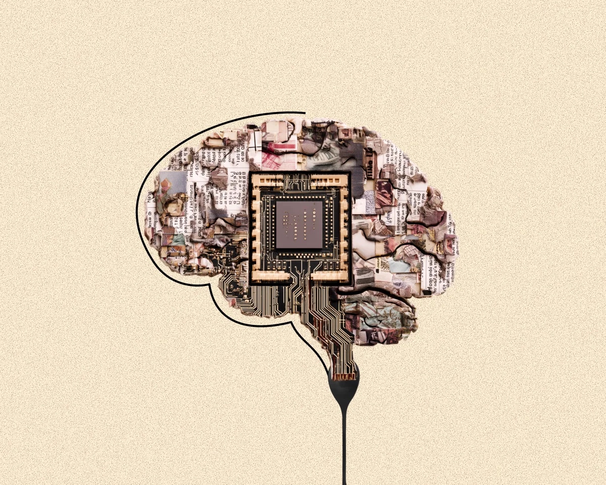
How will AI chips overcome the “memory wall”?
consumer GPU Traditionally, it has been built for video games and rendering. However, you can also tackle other tasks that require parallel computation.
For example, graphics processors can run PoW miners to mine cryptocurrencies, but competition from specialized rigs has pushed GPU farms into a niche market.
A similar story is happening with AI. Graphics cards are the backbone of neural networks. As the industry advances, the demand for dedicated AI hardware is increasing. ForkLog investigates the current state of this new wrap in the artificial intelligence race.
Optimize silicon for AI
There are several approaches to building specialized hardware for AI tasks.
Consumer GPUs are the starting point for specialization. Their superior ability in parallel matrix computations proved useful for deploying neural networks, especially deep learning, but there was plenty of room for improvement.
One of the main problems with running AI on the GPU is that large amounts of data must be constantly transferred between system memory and the GPU. These chores may take more time and energy than the useful calculations themselves.
Another problem stems from the versatility of GPUs. Its architecture supports a wide range of jobs, from graphics rendering to general-purpose computing, with some hardware blocks redundant for targeted AI workloads.
There are further restrictions on the data format. Historically, graphics processors have been tuned for FP32 (32-bit floating point numbers). Inference and training typically use lower precision formats such as 16-bit FP16 and BF16, or integer INT4 and INT8.
Nvidia H200 and B200
Some of our most popular products for inference and training (H200 chips and DGX B200 server systems) are essentially GPUs powered for data centers.
The core AI-oriented features of these accelerators are: tensor core, training model and batch inference.
To reduce data access latency, Nvidia includes a large amount of high-bandwidth memory (HBM) on the card. The H200 integrates 141 GB of HBM3e, delivering 4.8 TB/s. For B200, this number is even higher, depending on configuration.
tensor processing unit
By 2015, Google developed the Tensor Processing Unit (TPU), an ASIC built on systolic arrays for machine learning.
In traditional CPU and GPU architectures, each operation involves reading, processing, and writing intermediate data to memory.
The TPU streams data through an array of blocks, each performing mathematical operations and passing the results to the next block. Memory is used only at the beginning and end of the calculation sequence.
This approach still relies on external memory as a constraint, but spends less time and energy computing the AI than a non-dedicated GPU.
cerebrum
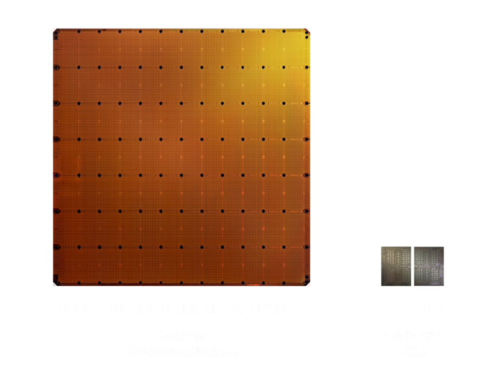
American company Cerebras has discovered a way to use an entire silicon wafer as a single processor, rather than dividing it into smaller chips.
The company introduced its first 300mm wafer-scale engine in 2019. In 2024, we released an improved WSE-3 with a 460mm die with 900,000 cores.
The Cerebras architecture places SRAM blocks right next to logic modules on the same wafer. Each core operates with its own 48KB of local memory to avoid contention with other cores.
According to the company, one WSE-3 is sufficient for many inference workloads. For larger jobs, multiple chips can be clustered.
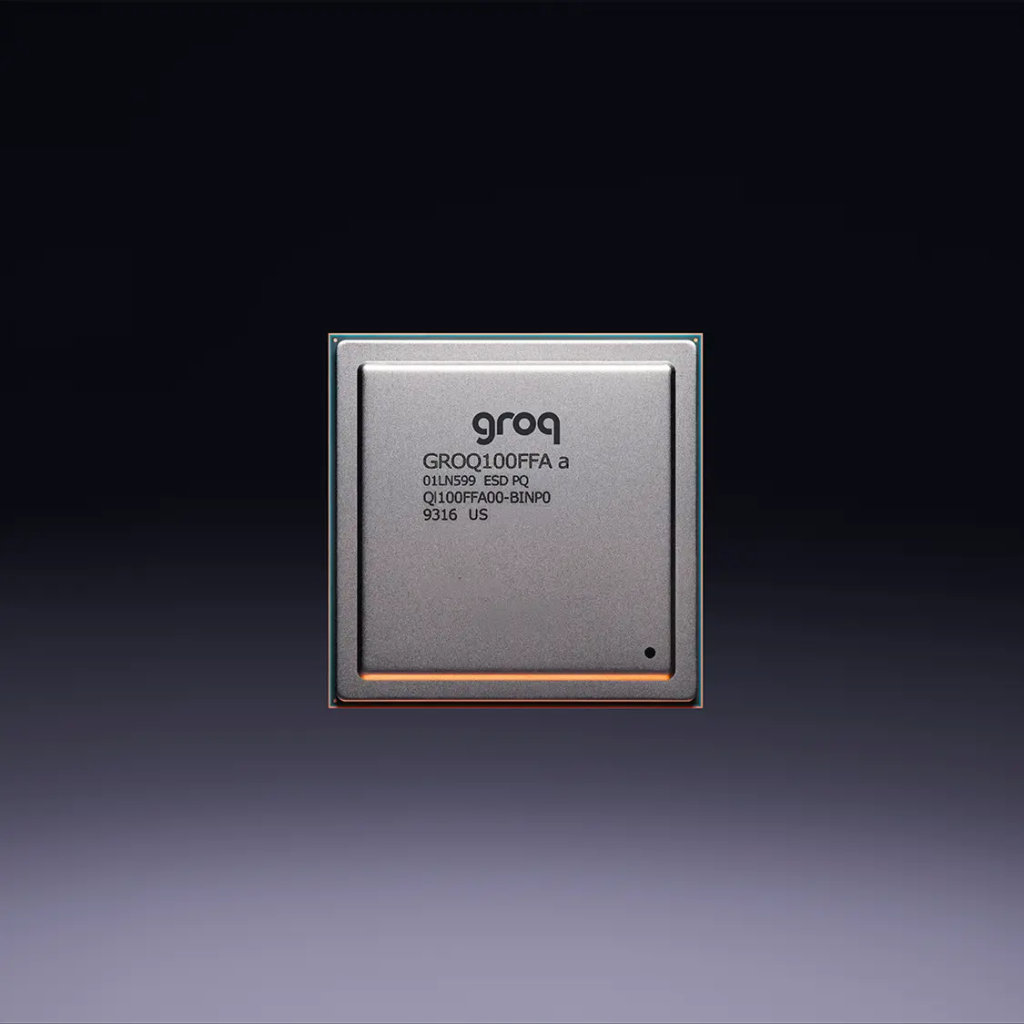
Groq LPU
Groq (not to be confused with xAI’s Grok) offers a unique inference ASIC built on the Language Processing Unit (LPU) architecture.
One of the key features of Groq’s chips is the optimization of sequential operations.
Inference generates tokens step by step. Each stage requires the completion of the previous stage. Under such constraints, performance depends more on the speed of a single stream than on the number of streams.
Unlike well-known general-purpose processors and some AI-specific devices, Groq does not assemble machine instructions on the fly. All operations are planned in advance in a kind of “schedule”, fixed at a certain moment of the processor’s work.
Like some other AI accelerators, LPUs combine logic and memory on a single die to minimize data movement.
Taras
All of the above assumes a high degree of programmability. The model and its weights are loaded into rewriteable memory. Operators can swap out for another model or make tweaks at any time.
With this approach, performance depends on memory availability, speed, and capacity.
Taalas went further and chose to wire a specific model with fixed weights directly into the chip at the transistor level.
What would normally be software becomes hardware, eliminating the need for a separate general-purpose data store and the associated costs.
For its first product, the HC1 inference card, the company used the open Llama 3.1 8B model.
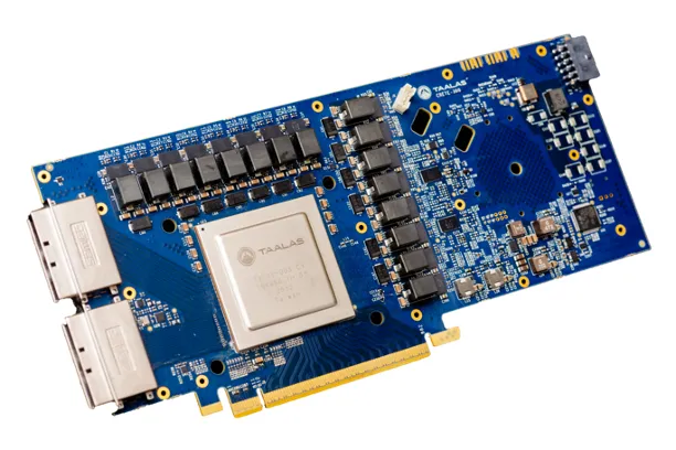
This card supports low bit precision up to 3-bit and 6-bit parameters for faster processing. According to Taalas, HC1 processes up to 17,000 tokens per second while being relatively inexpensive and using low power consumption.
The company touts performance improvements of thousands of times compared to GPUs on a cost and power basis.
However, the fundamental drawback of such hardwiring is that the model cannot be updated without replacing the chip.
Still, HC1 supports LoRA, which is a fine-tuning method. LLM By adding additional weights. With the right LoRA configuration, you can turn your model into a specialist in a particular field.
Another difficulty is the design and manufacturing process of such “physical models.” Developing ASICs is expensive and can take several years. This is a significant constraint in the rapidly changing AI market.
Taalas says he has developed a new way to generate processor architectures to address this. An automated system converts the model and set of weights into a finished chip design within a week.
According to the company’s own estimates, the production cycle from receiving a new, never-before-seen model to shipping the chips that incorporate it into hardware takes about two months.
The future of local inference
The new specialized AI chips will first be deployed in vast data center facilities to power pay-as-you-go cloud services. More radical options are no exception, even if they are “physical models” realized directly in silicon.
For consumers, engineering leaps will manifest as cheaper services and faster responses.
At the same time, simpler, cheaper, and more energy-efficient chips lay the foundation for widespread local inference.
Specialized AI chips are already in smartphones, laptops, security cameras, and even doorbells. These enable local processing with low latency, autonomy, and privacy.
Even at the expense of flexibility in model selection and replacement, radical optimizations can significantly expand the functionality that such devices can perform, allowing simple AI components to penetrate inexpensive mass-market products.
If most users begin to route queries to models that run on their local devices, this could reduce the strain on data center capacity and reduce the risk of overloading it. Perhaps then we won’t have to look for radical ways to scale computing, such as launching it into orbit.
Found a mistake? Select it and press CTRL+ENTER
ForkLog: держите руку на пульсе биткоин-индустрии!


